New electronic stickers to add sensor to all objects
The latest technology, like Internet of Things is intended to give us convenience and to make improvements in various sectors. However, to realize the ultimate vision behind the development of technology, we have to integrate various physical devices with digital systems. Recently, Virginia and Purdue University researchers have taken the challenge to connect any object to IoT very easily. They have relied on an innovative fabrication process to get the solution. Due to this fabrication technique, small, thinner filmed Electronic stickers circuits can be peeled off the surface.
This special technique enables an object in sensing the surrounding environment. The object also becomes easily controllable by using electronic stickers. You can now avoid several intricate manufacturing efforts.
Electronic stickers: More connectivity in the present world–
Nowadays, different objects, including the watches, machinery parts, Smartphone and buildings, have turned out to be the wireless sensors. It has caused the development of IoT network.
The present society is getting ready to link every object with Internet. This object may be your office item or furniture of your house. The technology, enabling the objects in interacting with one another, is also scaling up. Thus, the scientists’ latest fabrication technique is also one of those steps to meet the target.
The newly developed stickers will be able to trigger wireless interaction. Chi H. Lee, one of the assistant professors of Purdue University, has said that his team could tailor the sensor, and fit it to a drone. They could also move that drone system through various dangerous sites for the detection of gas leakage.
Electronic stickers: Peeling system in the new technique-
At present, you can find lots of electronic circuits, which are designed separately with a silicon component, one of the solid substrates. This silicon layer is capable of enduring the chemical-based printing and intense temperature. This temperature can cause damage to silicon. However, the process of manufacturing can hold the silicon layer fully.
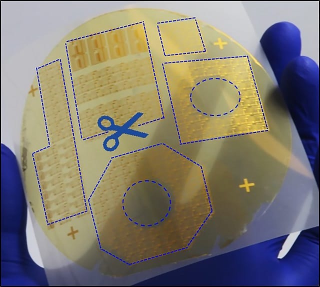
Now, let’s talk about the latest fabrication process of Lee, and this process is known as the transfer printing. The best fact is that it lowers the costs of manufacturing with the use of one silicon wafer for forming several thinner layers or films to hold the circuits. Under normal temperature, this film is easily removable.
There is a flexible layer of metal, like nickel, and this is placed between silicon and electronic film. That is why the process of peeling becomes simple with the application water.
Researchers, pasting the electronic stickers on various objects-
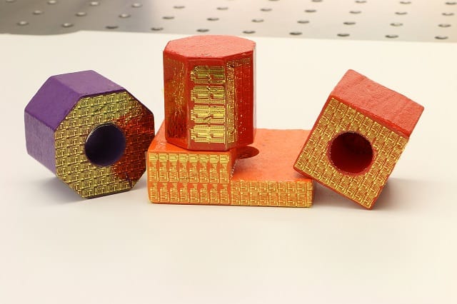
The scientists will cut the thin electronic film for pasting it on the surface of any object. This object will gain various electronic traits. For instance, they can place the electronic stickers on your guitar or on your flower vase. These simple objects can achieve the potential to sense the fluctuation of temperature. In case of the vase, this can affect the growth of plants.
Thus, the mechanical and biomedical engineers have made lots of efforts to deal with the electronic stickers. They have amazed us with their latest fabrication style.