MRAM variants are different types of Magnetoresistive Random Access Memory distinguished by how they switch magnetization in a Magnetic Tunnel Junction (MTJ).
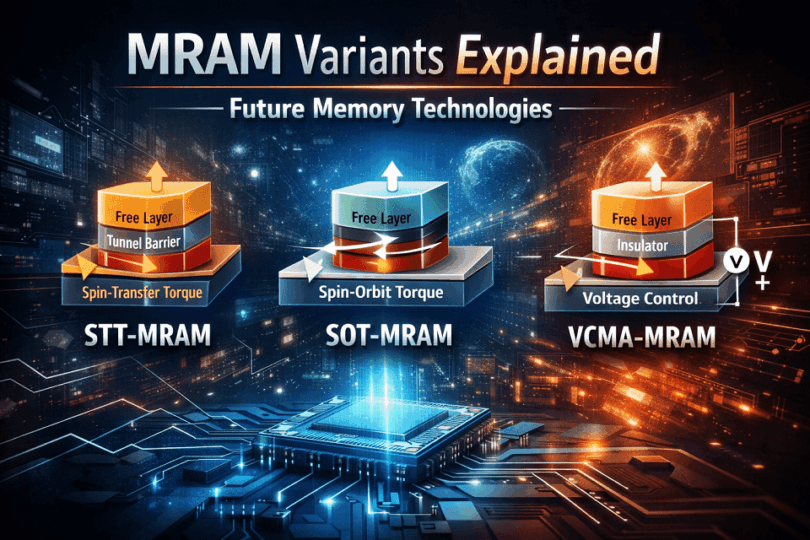
The main MRAM variants include Toggle MRAM, STT-MRAM, SOT-MRAM, VCMA-MRAM, and Thermally Assisted MRAM. Each type of MRAM is optimized for different trade-offs in speed, power, endurance, and scalability.
Introduction
What Is MRAM and Why Do Variants Exist
What Are MRAM Variants?
MRAM variants are different forms of Magnetoresistive Random Access Memory distinguished by how they switch magnetization inside a Magnetic Tunnel Junction (MTJ).
Each variant, such as STT-MRAM, SOT-MRAM, VCMA-MRAM, and Toggle MRAM, offers unique trade-offs in speed, power consumption, endurance, and scalability.
Magnetoresistive Random Access Memory (MRAM) is a non-volatile memory technology that stores data using magnetic states instead of electric charge. Each bit is represented by the relative magnetization of layers inside a Magnetic Tunnel Junction (MTJ). MTJ allows data to persist even when power is removed.
What Defines an MRAM Variant?
An MRAM variant is not defined by storage principle (all MRAM stores data magnetically), but by:
- Switching mechanism
- Current path during write
- Energy efficiency
- Scalability limits
- Reliability under repeated writes
At the heart of every MRAM variant lies the Magnetic Tunnel Junction (MTJ).
Why Do MRAM Variants Exist?
No single MRAM design can optimize speed, power, endurance, and density at the same time.
MRAM variants exist because different switching mechanisms are required for embedded systems, AI accelerators, low-power devices, and cache-level memory.
However, while the storage principle of MRAM is universal, the writing mechanism is not.
Switching magnetization reliably at nanometer scales involves complex trade-offs between speed, power, endurance, and scalability. As a result, multiple MRAM variants have emerged. Each Magnetoresistive Random Access Memory is engineered to solve a different bottleneck in magnetic switching. These variants differ not in what they store, but in how they write.
How MRAM Variants Are Classified
MRAM variants are classified based on their switching mechanism, current path, and device geometry.
The most common categories include field-induced switching, current-induced torque switching, voltage-controlled switching, and thermally assisted switching.
Why MRAM Variants Matter in Modern Memory Hierarchies
Modern computing systems no longer rely on a single type of memory. Instead, they use layered memory hierarchies from ultra-fast caches to dense main memory and persistent storage. No single MRAM design can optimally serve all these layers.
MRAM variants matter because:
- Cache-level memory prioritizes speed and endurance.
- Embedded systems demand low power and non-volatility.
- AI accelerators require fast, repeatable writes.
- Advanced nodes impose strict scaling and reliability limits.
Different MRAM variants address these needs by tailoring the switching physics. Switching physics enables MRAM to compete with, or complement SRAM, DRAM, and emerging memories in specific roles rather than as a one-size-fits-all solution.
How This Guide Is Structured
This guide takes a variant-first, physics-aware approach to MRAM. It begins by establishing the fundamental building blocks shared by all MRAM technologies. And then systematically explores each major variant based on how magnetization switching is achieved.
You will find:
- A clear explanation of what defines an MRAM variant.
- In-depth sections on Toggle, STT, SOT, VCMA, and Thermally Assisted MRAM.
- Geometry-based distinctions, such as in-plane vs perpendicular MRAM.
- Comparative analysis covering speed, power, endurance, and scalability.
- Context on where each MRAM variant fits in real-world systems.
The goal is not only to explain how MRAM variants work, but why they exist, and where each one makes the most sense in next-generation computing.
Fundamentals of MRAM Technology
What Is Magnetoresistive Random Access Memory (MRAM)?
Magnetoresistive Random Access Memory (MRAM) is a non-volatile memory technology that stores information using magnetic states rather than electrical charge. Each memory bit is implemented using a nanoscale structure called a Magnetic Tunnel Junction (MTJ). In a Magnetic Tunnel Junction, data is encoded by the relative orientation of magnetic layers.
Magnetic Tunnel Junction (MTJ)
MTJ Structure
- Free layer – switchable magnetization
- Tunnel barrier – usually MgO (~1 nm)
- Pinned (reference) layer – fixed magnetization
Resistance States
- Parallel (P) → Low resistance → Logic “0”
- Anti-parallel (AP) → High resistance → Logic “1”
All MRAM variants differ only in how the free layer is switched.
Unlike conventional memories, MRAM does not require continuous power to retain data. The information is stored in the magnetization direction of a ferromagnetic layer. The ferromagnetic layer makes MRAM inherently resistant to power loss, leakage current, and many forms of environmental stress. This combination of non-volatility, speed, and endurance positions MRAM as a candidate for bridging the long-standing gap between working memory and storage.
At its core, MRAM belongs to the broader class of spintronic devices. It exploits the electron’s spin in addition to its charge. This spin-based operation is the foundation on which all MRAM variants are built.
Why MRAM Is Different from Charge-Based Memory
Traditional memories such as SRAM, DRAM, and Flash memory store data by accumulating or removing electrical charge. While this approach has scaled well for decades, it comes with fundamental limitations that become more severe at advanced nodes.
MRAM vs Charge-Based Memory Technologies
| Feature | MRAM (Magnetoresistive RAM) | Charge-Based Memory (SRAM, DRAM, Flash) |
| Data storage principle | Magnetic orientation of layers in an MTJ | Electrical charge stored in capacitors or transistors |
| Volatility | Non-volatile | SRAM & DRAM are volatile; Flash is non-volatile |
| Data retention | Retains data without power | Volatile memories lose data without power |
| Refresh requirement | No refresh required | DRAM requires periodic refresh |
| Standby power consumption | Near zero | SRAM and DRAM consume standby power |
| Write endurance | Very high (10¹²–10¹⁵ cycles) | Limited for Flash; high for SRAM/DRAM |
| Write speed | Fast (nanoseconds) | SRAM fast; DRAM moderate; Flash slow |
| Scalability limits | Thermal stability and magnetic volume | Charge leakage and capacitor scaling |
| Radiation sensitivity | Naturally radiation-tolerant | Susceptible to soft errors |
| Data integrity on power loss | Instant and inherent | Requires backup mechanisms |
| Primary failure mode | Magnetic instability at extreme scaling | Charge leakage and wear-out |
MRAM differs in several fundamental ways:
- Retention is intrinsic and does not depend on refresh cycles.
- State is preserved instantly during power loss.
- MRAM eliminates refresh overhead
- Charge leakage dominates advanced DRAM scaling
- Endurance favors MRAM for write-heavy workloads
Charge-based memories face a constant trade-off between speed, volatility, and power consumption. MRAM avoids many of these compromises because the magnetic state of an MTJ remains stable without energy input. This is why MRAM is often discussed as a universal memory candidate, even though practical implementations rely on multiple variants rather than a single design.
Basic Read and Write Operations in MRAM
Although MRAM variants differ in how they write data. However, the read operation is largely similar across all types.
Read operation:
A small sensing current passes through the MTJ. The resistance depends on whether the free layer magnetization is parallel or anti-parallel to the reference layer. This resistance difference, known as tunneling magnetoresistance (TMR), is detected by sense amplifiers to determine the stored bit.
Write operation:
Writing data involves changing the magnetization direction of the free layer. This is where MRAM variants diverge:
- Some use spin-polarized current flowing through the MTJ.
- Others rely on spin currents generated in adjacent layers.
- Experimental approaches use electric fields or thermal assistance.
The key challenge in MRAM writing is achieving fast, reliable switching without disturbing neighboring cells or degrading the MTJ over time. How each variant addresses this challenge defines its performance envelope and application domain.
Key Performance Metrics Used to Classify MRAM Variants
MRAM variants are not classified arbitrarily. They are evaluated and differentiated using a consistent set of device- and system-level performance metrics.
The most important metrics include:
- Switching speed
- Determines suitability for cache, working memory, or storage-class roles.
- Write energy and power consumption
- Critical for embedded systems, mobile devices, and large memory arrays.
- Endurance
- Measured in write cycles, MRAM typically exceeds 10¹² cycles. However, variants differ in long-term reliability.
- Thermal stability and retention
- Defines how long data can be stored without errors, especially at small dimensions.
- Scalability
- Indicates whether a variant can function reliably below 20 nm and beyond.
- Read and write disturb susceptibility
- Affects array-level reliability and error correction overhead.
No single MRAM variant optimizes all these parameters simultaneously. Instead, each variant prioritizes a specific subset. That is the reason why multiple MRAM designs coexist rather than converging into a single universal architecture.
Magnetic Tunnel Junction (MTJ): The Core of All MRAM Variants
The Magnetic Tunnel Junction is the fundamental building block that determines how MRAM stores, reads, and retains data.
All MRAM variants differ in how they interact with the MTJ, but not in the MTJ’s core storage principle.

Layer Structure of an MTJ
An MTJ is a carefully engineered multilayer stack designed to control electron spin and tunneling behavior.
Its layer composition directly influences switching reliability, retention, and scalability.
An MTJ is a nanoscale multilayer stack engineered to control electron spin transport with extreme precision. However, implementations vary slightly across vendors and variants, while the essential structure remains consistent.
A typical MTJ consists of:
- Free layer
- A free layer is a ferromagnetic layer whose magnetization can be switched during write operations.
- Tunnel barrier
- Tunnel Barrier is an ultra-thin insulating layer. It is most commonly magnesium oxide (MgO), typically ~1 nm thick.
- Reference (pinned) layer
- A pinned layer is a ferromagnetic layer with fixed magnetization, stabilized using exchange coupling.
- Capping and seed layers
- Used to control crystallinity, anisotropy, and interface quality.
In modern MRAM, the MTJ stack is usually engineered with perpendicular magnetic anisotropy (PMA). That significantly improves scalability and thermal stability compared to older in-plane designs.
Spin-Dependent Tunneling and TMR Ratio
MRAM readout relies on the quantum-mechanical dependence of electron tunneling on spin orientation.
This effect produces the tunneling magnetoresistance (TMR) signal that enables fast and reliable sensing.
The operation of an MTJ is governed by spin-dependent quantum tunneling. Although the tunnel barrier is electrically insulating, electrons can tunnel through it if their quantum wavefunctions align appropriately.
Crucially, the tunneling probability depends on the relative spin orientation between the free and reference layers. When spins are aligned, tunneling is more efficient; when misaligned, tunneling is suppressed.
This behavior gives rise to the Tunneling Magnetoresistance (TMR) ratio. The TMR ratio is defined as the relative change in resistance between magnetic states.
In practical terms:
- Higher TMR improves read margin.
- A larger read margin reduces sensing errors.
- Strong TMR enables lower read currents.
Modern MgO-based MTJs achieve TMR ratios exceeding 150–200%, which is a key reason MRAM became commercially viable.
Parallel vs Anti-Parallel Resistance States
Binary data in MRAM is represented by two stable magnetic configurations of the MTJ.
These states correspond to distinct resistance levels that can be read without disturbing stored data.
Data in MRAM is stored using two stable resistance states of the MTJ:
- Parallel (P) state
- In Parallel state, the magnetization of the free layer aligns with the reference layer, resulting in low resistance.
- Anti-parallel (AP) state
- In AP state, the magnetizations oppose each other, resulting in high resistance.
These two states represent binary information and are inherently non-volatile. Once written, the state persists without power because it is stabilized by magnetic anisotropy rather than stored charge.
From a system perspective, the clear separation between P and AP resistance states enables:
- Fast read access
- Robust sensing at low voltages
- High immunity to soft errors
Thermal Stability Factor (Δ) and Data Retention
Data retention in MRAM depends on how resistant the magnetic state is to thermal fluctuations.
The thermal stability factor (Δ) quantifies this resistance and becomes critical as MTJs shrink.
One of the most critical parameters in MRAM design is the thermal stability factor. The thermal stability factor is commonly denoted as Δ (Delta). It quantifies how resistant the stored magnetic state is to spontaneous thermal flipping.
Δ is determined by:
- Magnetic anisotropy energy
- Volume of the free layer
- Operating temperature
For reliable non-volatile memory, Δ must be sufficiently high, typically ≥ 60 for 10-year data retention at room temperature. As device dimensions shrink, maintaining this stability becomes increasingly difficult because the magnetic volume decreases.
This creates a fundamental trade-off:
- Smaller MTJs improve density
- Larger MTJs improve retention
MRAM variants differ in how they manage this balance, particularly when pushing toward sub-10 nm technology nodes.
Scaling Limits of MTJ Devices
Scaling MRAM is ultimately limited by fundamental magnetic and material constraints within the MTJ.
These limits explain why new MRAM variants continue to emerge.
While MRAM scales better than many alternative non-volatile memories, MTJ scaling is not unlimited. Several physical and manufacturing constraints emerge at advanced nodes.
Key scaling challenges include:
- Reduced thermal stability at small dimensions.
- Increased variability in MTJ resistance.
- Tunnel barrier thickness control at atomic scales.
- Write current density limits.
- Reliability degradation under repeated switching.
Perpendicular MTJs mitigate some of these issues, but not all. As a result, modern MRAM research focuses heavily on new switching mechanisms such as spin-orbit torque and voltage-controlled anisotropy. This new switching mechanisms help to decouple scaling from excessive current stress.
These limits are the primary reason why MRAM variants exist at all. Each variant represents a different strategy to push MTJ-based memory further along the scaling curve without sacrificing reliability or performance.
How MRAM Variants Are Classified
MRAM variants differ in how they write data magnetically, not in how they store it.
MRAM variants are classified based on how magnetization is switched, how current flows during write operations, and how the MTJ is physically engineered.
These classification axes reflect real device constraints and explain why no single MRAM architecture dominates all applications.
Classification Based on Switching Mechanism
The switching mechanism defines how the free layer magnetization is reversed during a write operation.
This is the most fundamental distinction between MRAM variants because it directly determines write speed, energy, reliability, and scalability.
From a physics perspective, MRAM switching mechanisms fall into several broad categories:
- Magnetic-field-induced switching
- Used in early Toggle MRAM, where external magnetic fields flip the free layer. This approach suffers from poor scalability and high power consumption.
- Spin-transfer torque (STT) switching
- A spin-polarized current passes through the MTJ and transfers angular momentum to the free layer. This is the dominant mechanism in commercially deployed MRAM today.
- Spin-orbit torque (SOT) switching
- Spin currents generated in an adjacent heavy metal layer exert torque on the free layer without stressing the tunnel barrier. It is enabling ultra-fast and durable operation.
- Voltage-controlled magnetic anisotropy (VCMA) switching
- An electric field modulates interfacial magnetic anisotropy. VCMA is allowing magnetization switching with minimal current and extremely low energy.
- Thermally assisted switching
- Local heating temporarily lowers the energy barrier. The thermally assisted switching is making magnetization reversal easier under reduced current or field.
Each of these mechanisms addresses a different bottleneck in MTJ switching. That is why multiple MRAM variants continue to coexist.
Classification Based on Current Path
How electrical current flows during write operations has major implications for reliability and device lifetime.
MRAM variants are often grouped by whether the write current passes through the tunnel barrier or bypasses it entirely.
Two dominant current-path architectures are used:
- Two-terminal MRAM
- The same paths are used for read and write operations. STT-MRAM falls into this category, where write current flows directly through the MTJ. This enables compact cell sizes but introduces tunnel barrier stress.
- Three-terminal MRAM
- Read and write paths are separated. SOT-MRAM is the most prominent example, where write current flows in-plane through a heavy metal layer, while read current passes through the MTJ.
The trade-off is clear:
- Two-terminal designs favor density and simplicity
- Three-terminal designs favor speed, endurance, and reliability
This classification is especially important when evaluating MRAM for cache-level or high-write-intensity workloads.
Classification Based on Device Geometry
The orientation of magnetization relative to the device plane strongly influences scalability and retention.
Geometry-based classification focuses on how the MTJ is magnetically and physically structured.
The two primary geometries are:
- In-plane MRAM
- Magnetization lies parallel to the wafer surface. While simpler to fabricate, this geometry suffers from poor scaling and limited thermal stability at small dimensions.
- Perpendicular MRAM (pMTJ-based)
- Magnetization is oriented perpendicular to the wafer surface. That is enabled by strong interfacial anisotropy. This geometry provides superior scalability and retention.
Modern MRAM variants universally adopt perpendicular MTJs because they allow:
- Higher thermal stability at smaller volumes.
- Lower switching current densities.
- Better compatibility with advanced CMOS nodes.
Geometry is no longer a differentiator among modern variants. However, it is a prerequisite for their viability.
Classification Based on Power and Endurance Trade-offs
Different MRAM variants optimize different points on the power–endurance–speed spectrum.
This classification is critical from a system-design perspective.
Broadly:
- High-endurance variants (such as SOT-MRAM) target cache and accelerator workloads with frequent writes.
- Low-power variants (such as VCMA-MRAM) are aimed at energy-constrained environments.
- Balanced variants (such as STT-MRAM) are optimized for embedded and general-purpose use.
Key trade-offs include:
- Lower write energy often comes at the cost of reduced thermal stability.
- Higher endurance may require larger cells or additional transistors.
- Faster switching can increase instantaneous power density.
These trade-offs explain why MRAM adoption is application-specific rather than universal, and why future memory systems are likely to integrate multiple MRAM variants rather than standardize on one.
Why This Classification Matters
By organizing MRAM variants along these four dimensions, such as switching mechanism, current path, geometry, and power–endurance balance, it becomes possible to compare technologies on equal footing. This framework also clarifies how emerging MRAM designs fit into the broader memory landscape.
Toggle MRAM (Field-Induced MRAM)
Toggle MRAM is the earliest practical form of Magnetoresistive RAM and the foundation on which all modern MRAM variants were built.
Although it is no longer commercially relevant, understanding Toggle MRAM is important because it highlights the fundamental challenges that later variants were designed to overcome.
Historical Background and Early Development
Toggle MRAM emerged in the late 1990s and early 2000s as the first scalable magnetic random access memory technology.
It evolved from earlier anisotropic and giant magnetoresistance memories once magnetic tunnel junctions became manufacturable.
Early research demonstrated that magnetic bits could be written and read reliably, even in harsh environments. This made Toggle MRAM attractive for:
- Aerospace and defense systems
- Industrial controllers
- Radiation-tolerant electronics
At the time, Toggle MRAM represented a major breakthrough because it combined non-volatility with true random access. That is something Flash memory could not provide.
Magnetic Field-Based Switching Mechanism
Toggle MRAM writes data by generating localized magnetic fields that flip the magnetization of the free layer.
This is achieved using two orthogonal current-carrying lines: a word line and a bit line.
When both lines are energized simultaneously:
- Their magnetic fields overlap at the selected cell.
- The combined field exceeds the switching threshold.
- The free layer magnetization toggles to the opposite state.
The key characteristic of this mechanism is that the magnetic field does not directly depend on electron spin transport, unlike later torque-based approaches. While conceptually simple, this method introduces fundamental inefficiencies at small scales.
Write Selectivity and the Half-Select Problem
One of the most serious challenges in Toggle MRAM is the half-select problem.
Cells that lie along either the word line or bit line experience partial magnetic fields during a write operation.
This creates several risks:
- Unintended disturbance of neighboring cells.
- Increased error probability at high densities.
- Need for carefully tuned switching thresholds.
To mitigate these issues, Toggle MRAM requires precise control of current amplitudes and timing. That becomes increasingly difficult as arrays grow larger. This limitation severely constrained the achievable memory density.
Scalability and Power Limitations
Field-induced switching scales poorly as device dimensions shrink.
As MRAM cells become smaller, generating a sufficiently strong magnetic field requires disproportionately higher current density.
Major limitations include:
- High write current and power consumption.
- Significant Joule heating.
- Poor compatibility with advanced CMOS nodes.
- Crosstalk between adjacent cells.
Below the roughly 90 nm technology node, these factors made Toggle MRAM impractical for mainstream semiconductor manufacturing.
Why Toggle MRAM Became Obsolete
Toggle MRAM was ultimately replaced because its write mechanism could not scale with semiconductor technology.
While reliable and robust, it could not compete with torque-based MRAM variants that offered:
- Lower write energy
- Better scalability
- Higher integration density
- Improved write selectivity
Today, Toggle MRAM survives only as a historical reference point. Its shortcomings directly motivated the development of Spin-Transfer Torque (STT-MRAM), which eliminated magnetic field generation entirely and enabled the next era of MRAM innovation.
Key Takeaway
Toggle MRAM proved that magnetic memory was feasible, but also demonstrated why magnetic fields are unsuitable for nanoscale memory switching. Every modern MRAM variant exists as a response to the limitations exposed by this first generation. It is an Obsolete / Legacy Technology.
Spin-Transfer Torque MRAM (STT-MRAM)
Spin-Transfer Torque MRAM (STT-MRAM) is the first MRAM variant to achieve large-scale commercial deployment.
It replaces magnetic-field-based switching with a current-driven spin mechanism. STT-RAM enables much better scalability, lower power consumption, and full compatibility with modern CMOS processes.
Physical Principle of Spin-Transfer Torque
Spin-transfer torque is a quantum-mechanical effect in which a spin-polarized current transfers angular momentum to a magnetic layer.
When electrons flow through a ferromagnetic material, their spins become aligned with the magnetization of that layer.
As this spin-polarized current enters the free layer of the MTJ:
- The electron spins interact with the local magnetic moments.
- Angular momentum is transferred.
- A torque is exerted on the free-layer magnetization.
If the torque exceeds a critical threshold, the magnetization switches direction. This mechanism eliminates the need for external magnetic fields and allows switching to occur directly at the nanoscale.
Current-Induced Switching Through the MTJ
In STT-MRAM, the write current flows directly through the Magnetic Tunnel Junction.
This two-terminal architecture uses the same vertical current path for both read and write operations.
Key characteristics of this approach include:
- Compact cell size and high density.
- Simple integration with CMOS logic.
- Strong coupling between current and switching probability.
However, because the write current passes through the ultra-thin MgO tunnel barrier, the MTJ experiences electrical stress during every write cycle. This creates a fundamental trade-off between write speed, power, and long-term reliability.
Perpendicular STT-MRAM (p-STT-MRAM)
Modern STT-MRAM implementations rely almost exclusively on perpendicular magnetic tunnel junctions (pMTJs).
In this geometry, magnetization is oriented perpendicular to the wafer surface rather than in-plane.
Perpendicular STT-MRAM offers several critical advantages:
- Lower switching current at small dimensions.
- Improved thermal stability for a given cell size.
- Better scalability below 20 nm technology nodes.
The combination of spin-transfer torque and perpendicular magnetic anisotropy is what makes STT-MRAM viable as a dense embedded memory technology today.
Read Disturb and Write Reliability Challenges
Because STT-MRAM uses the same current path for reading and writing, read disturb is a central reliability concern.
Although read currents are lower than write currents, repeated reads can occasionally induce unintended switching, especially at scaled nodes.
Additional reliability challenges include:
- Tunnel barrier degradation due to high current density.
- Variability in switching thresholds across cells.
- Trade-offs between fast writes and long retention.
To address these issues, commercial STT-MRAM designs rely on careful circuit-level optimization, error correction, and conservative operating margins.
Endurance, Retention, and Switching Speed
STT-MRAM offers a powerful balance between endurance, retention, and performance.
This balance is a major reason for its commercial success.
Typical characteristics include:
- Endurance: 10¹² to 10¹⁵ write cycles
- Retention: 10 years at elevated temperatures
- Switching speed: A few nanoseconds, depending on write current
While STT-MRAM is not as fast as SRAM, it dramatically outperforms Flash and other non-volatile memories in both speed and endurance.
Commercial Adoption and Embedded MRAM Use Cases
STT-MRAM is currently the most widely deployed MRAM variant in the semiconductor industry.
Its combination of non-volatility, endurance, and CMOS compatibility makes it especially attractive for embedded applications.
Common use cases include:
- Embedded non-volatile memory in microcontrollers.
- Automotive electronics require instant-on behavior.
- Industrial and IoT devices with frequent power cycling.
- Secure memory for firmware and cryptographic keys.
Rather than replacing all existing memories, STT-MRAM is increasingly used to replace embedded Flash and EEPROM, where its advantages are most pronounced.
Key Takeaway
STT-MRAM represents the transition of MRAM from a laboratory concept to a production-ready technology. Its limitations, particularly tunnel barrier stress and read disturb, are precisely what motivate the development of next-generation variants such as SOT-MRAM, which we will examine next.
Spin-Orbit Torque MRAM (SOT-MRAM)
Spin-Orbit Torque MRAM (SOT-MRAM) is widely regarded as the next evolutionary step beyond STT-MRAM.
It was developed to overcome the reliability and speed limitations of current-induced switching through the MTJ by separating the write and read paths at the device level.
Spin Hall Effect and Rashba Effect in SOT Devices
SOT-MRAM relies on relativistic spin–orbit interactions to generate spin currents without passing charge through the tunnel barrier.
Two closely related physical phenomena are responsible for this behavior.
The Spin Hall Effect (SHE) occurs in heavy metals such as tantalum, tungsten, or platinum. When a charge current flows through these materials, electrons with opposite spins deflect in opposite transverse directions, creating a pure spin current.
The Rashba effect arises at interfaces with strong structural inversion asymmetry, where spin–orbit coupling produces interfacial spin accumulation.
In SOT-MRAM:
- A lateral charge current flows through a heavy metal underlayer.
- A transverse spin current is generated via SHE (and sometimes Rashba contributions).
- The spin current exerts torque on the free magnetic layer.
This mechanism enables ultra-fast and efficient magnetization switching without electrical stress on the tunnel barrier.
Three-Terminal MRAM Architecture
SOT-MRAM uses a three-terminal device architecture that cleanly separates read and write operations.
This structural difference is central to its performance advantages.
In a typical SOT-MRAM cell:
- One terminal is used for reading through the MTJ.
- Two separate terminals are used for writing through the heavy metal channel.
This separation provides:
- Elimination of tunnel barrier degradation during writes.
- Strong suppression of read disturbs.
- Independent optimization of read and write currents.
While this architecture improves reliability and speed, it also introduces new challenges related to area efficiency.
Advantages over STT-MRAM
SOT-MRAM directly addresses the two major weaknesses of STT-MRAM: write reliability and speed.
Because the write current bypasses the tunnel barrier, several critical improvements are achieved.
Key advantages include:
- Sub-nanosecond switching capability
- Endurance exceeding 10¹⁵ write cycles
- Near-zero write-induced MTJ degradation
- Improved write determinism and reduced variability
These properties make SOT-MRAM particularly attractive for workloads involving frequent and latency-sensitive writes, where STT-MRAM begins to show stress-related limitations.
Cell Size and Area Overhead Challenges
The main drawback of SOT-MRAM lies in its larger cell size.
The three-terminal architecture requires additional transistors and routing compared to two-terminal STT-MRAM cells.
This leads to:
- Increased cell area
- Lower memory density
- Higher fabrication complexity
As a result, SOT-MRAM is less suitable for large, dense memory arrays where cost per bit is critical. Ongoing research focuses on reducing this overhead through device scaling, novel materials with higher spin Hall efficiency, and optimized layouts.
High-Speed and Cache-Level Applications
SOT-MRAM is optimized for speed and endurance rather than density.
This positions it well for use cases that traditionally rely on SRAM.
Potential applications include:
- Last-level caches in processors
- Write-intensive buffers in AI accelerators
- High-speed scratchpad memory
- Radiation-tolerant cache memory in aerospace systems
Although SOT-MRAM is unlikely to replace SRAM across all cache levels. The SOT-MRAM offers a compelling alternative where non-volatility and endurance provide system-level benefits.
Current Commercial and Pre-Commercial Status
SOT-MRAM is transitioning from advanced research to early commercial deployment.
While not yet as widespread as STT-MRAM, it has moved beyond the laboratory stage.
Current status highlights:
- Demonstrated compatibility with advanced CMOS nodes.
- Early pilot production and limited-volume products.
- Strong interest in high-performance and specialized markets.
Most industry roadmaps view SOT-MRAM as a complementary technology rather than a direct replacement for STT-MRAM, with each serving distinct roles in future heterogeneous memory hierarchies.
Key Takeaway
SOT-MRAM represents a fundamental architectural shift in MRAM design by decoupling write operations from the tunnel barrier. Its unmatched speed and endurance make it ideal for cache-level and high-performance applications, even though density and cost challenges currently limit its broader adoption.
Voltage-Controlled Magnetic Anisotropy MRAM (VCMA-MRAM)
Voltage-Controlled Magnetic Anisotropy MRAM (VCMA-MRAM) represents a shift from current-driven to electric-field-driven switching in magnetic memory.
Its goal is to dramatically reduce write energy by manipulating magnetic properties using voltage rather than high current density.
Concept of Electric-Field-Driven Switching
VCMA-MRAM switches magnetization by applying an electric field across the MTJ instead of driving a large current through it.
When a voltage is applied across the tunnel barrier, it modifies the magnetic anisotropy of the free layer at the atomic scale.
In practical terms:
- The energy barrier separating magnetic states is temporarily reduced.
- Magnetization switching becomes easier.
- Only a small assisting current or thermal fluctuation is required.
This approach directly targets the primary weakness of STT-MRAM: write energy consumption.
Interfacial Anisotropy Modulation in MgO-Based MTJs
The VCMA effect arises from changes in interfacial electronic structure at the ferromagnet–MgO interface.
In CoFeB/MgO MTJs, applying an electric field alters orbital hybridization and spin–orbit coupling at the interface.
This leads to:
- Modulation of perpendicular magnetic anisotropy.
- Reversible tuning of the energy landscape.
- Strong sensitivity to interface quality and atomic order.
Because VCMA is an interfacial phenomenon, its effectiveness depends heavily on materials engineering and fabrication precision, more so than in torque-based MRAM variants.
Energy Efficiency Advantages
The primary advantage of VCMA-MRAM is its exceptionally low switching energy.
By reducing or eliminating high write currents, VCMA-based switching minimizes Joule heating and power dissipation.
Key energy benefits include:
- Switching energies in the femtojoule range
- Reduced electromigration stress
- Improved energy efficiency for dense arrays
These properties make VCMA-MRAM particularly attractive for battery-powered and energy-constrained systems, as well as future ultra-dense memory architectures.
Thermal Stability and Reliability Constraints
Reducing the magnetic energy barrier introduces serious challenges for data retention and reliability.
While VCMA facilitates easier switching, it also risks making the stored state more susceptible to thermal noise.
Major constraints include:
- Difficulty maintaining high thermal stability (Δ) at small dimensions.
- Increased sensitivity to temperature variations.
- Greater impact of process variability.
Balancing low-energy switching with long-term data retention remains one of the central challenges preventing VCMA-MRAM from near-term commercialization.
Research Progress and Experimental Results
VCMA-MRAM has shown promising results in laboratory demonstrations. However, it remains largely experimental.
Research has achieved measurable anisotropy modulation and voltage-assisted switching in scaled MTJs.
Recent progress includes:
- Demonstration of voltage-assisted switching at reduced current.
- Improved interfacial engineering to enhance VCMA coefficients.
- Integration of VCMA effects with perpendicular MTJ structures.
However, reproducibility, yield, and long-term reliability under real operating conditions are still open research questions.
Long-Term Scalability Potential
VCMA-MRAM offers one of the most promising pathways for scaling MRAM beyond current limits.
Because switching energy does not scale directly with current density, VCMA-based approaches could remain viable at deeply scaled nodes.
Long-term potential includes:
- Ultra-dense non-volatile memory arrays.
- Hybrid VCMA–STT or VCMA–SOT architectures.
- Integration into low-power neuromorphic and in-memory computing systems.
While VCMA-MRAM is unlikely to replace existing MRAM variants in the short term, it plays a crucial role in shaping the future research roadmap of magnetic memory.
Key Takeaway
VCMA-MRAM challenges the assumption that magnetic memory must rely on high current to switch states. Its success depends on whether materials science and device engineering can reconcile ultra-low energy switching with robust thermal stability at scale.
Thermally Assisted MRAM (TA-MRAM)
Thermally Assisted MRAM (TA-MRAM) introduces controlled heating into the write process to improve switching selectivity and reliability.
Rather than relying solely on magnetic fields or spin torques, TA-MRAM temporarily lowers the magnetic energy barrier before switching the bit.
Motivation for Thermal Assistance
As MRAM devices scale down, reliably switching a single target cell without disturbing its neighbors becomes increasingly difficult.
High magnetic anisotropy is needed for long data retention. However, it also raises the energy required for writing.
Thermal assistance was introduced to address this conflict:
- Heating reduces magnetic coercivity.
- Lower energy barriers enable easier switching.
- Write selectivity improves without sacrificing retention.
TA-MRAM represents an intermediate strategy between field-driven and torque-driven MRAM variants.
Heating-Assisted Write Mechanism
TA-MRAM writes data by locally heating the MTJ during the write operation.
The elevated temperature temporarily reduces the magnetic anisotropy of the free layer.
A typical write cycle involves:
- Applying a short heating pulse to the selected cell.
- Reducing the switching energy barrier.
- Using a magnetic field or current to set the desired state.
- Allow the cell to cool and stabilize.
The heating is highly localized in time and space. But it still introduces additional complexity compared to purely electrical switching.
Benefits of Write Selectivity
Thermal assistance improves write selectivity by confining switching to the intended cell.
Only the heated MTJ experiences a sufficiently reduced energy barrier, while neighboring cells remain stable.
This leads to:
- Reduced half-select errors.
- Lower risk of unintended switching.
- Improved reliability in dense arrays.
These benefits made TA-MRAM attractive for scenarios where write precision is more critical than raw speed or energy efficiency.
Performance and Power Trade-Offs
The advantages of thermal assistance come with clear performance and power penalties.
Generating and dissipating heat requires additional energy and limits switching speed.
Key trade-offs include:
- Slower write times due to heating and cooling cycles.
- Higher overall energy consumption.
- Increased thermal management complexity.
- Potential impact on device lifetime.
As a result, TA-MRAM is generally less competitive than STT-MRAM or SOT-MRAM for mainstream applications.
Practical and Niche Use Cases
TA-MRAM is primarily suited for specialized applications rather than mass-market memory products.
Its strengths align with environments where reliability and selectivity outweigh density and speed.
Typical niche use cases include:
- Radiation-hardened memory systems.
- Industrial and aerospace electronics.
- Legacy systems transitioning from field-driven MRAM.
In modern memory roadmaps, TA-MRAM is often viewed as a transitional or complementary technology rather than a long-term solution.
Key Takeaway
TA-MRAM demonstrates how thermal effects can be leveraged to improve magnetic switching reliability. However, its added complexity and energy cost limit its role to niche applications, as more efficient torque- and voltage-based MRAM variants continue to mature.
Geometry-Based MRAM Variants
Beyond switching mechanisms, MRAM variants are also defined by the geometric orientation of magnetization within the MTJ.
Device geometry strongly influences scalability, thermal stability, switching efficiency, and long-term reliability.
In-Plane Magnetized MRAM
In-plane MRAM stores data using magnetization oriented parallel to the wafer surface.
This was the dominant geometry in early MRAM implementations due to its simpler fabrication and well-understood magnetic behavior.
Key characteristics include:
- Shape anisotropy dominates magnetic stability.
- Switching requires relatively large currents or magnetic fields.
- Thermal stability decreases rapidly as device dimensions shrink.
While in-plane MRAM demonstrated reliable operation at larger feature sizes, it faces severe limitations below roughly 60–90 nm. That makes it unsuitable for modern high-density memory arrays.
Perpendicular Magnetic Anisotropy (pMTJ)
Perpendicular MRAM uses magnetization oriented perpendicular to the plane of the wafer. That is enabled by strong interfacial magnetic anisotropy.
This geometry is realized using carefully engineered ferromagnet–MgO interfaces.
In pMTJ-based MRAM:
- Thermal stability scales more favorably with size.
- Switching current density is reduced.
- Device-to-device variability is improved.
Perpendicular magnetic anisotropy is now a foundational requirement for all advanced MRAM variants, including STT-MRAM, SOT-MRAM, and VCMA-MRAM.
Why Perpendicular MRAM Dominates Modern Designs
Perpendicular MRAM dominates because it resolves the fundamental scaling conflict between retention and density.
Unlike in-plane devices, pMTJs maintain sufficient energy barriers even as lateral dimensions shrink.
Key reasons for dominance include:
- Higher thermal stability at small volumes.
- Compatibility with sub-20 nm CMOS nodes.
- Lower write energy requirements.
- Improved read margin and sensing reliability.
From an industry perspective, the shift to perpendicular MRAM was the single most important enabler of MRAM commercialization.
Scaling Below 10 nm: Opportunities and Risks
Scaling MRAM below 10 nm introduces both exciting opportunities and serious physical risks.
At these dimensions, interfacial and quantum effects become dominant.
Opportunities include:
- Extremely high memory density.
- Potential integration into logic-level memory.
- Enhanced suitability for in-memory computing.
However, significant risks remain:
- Rapid loss of thermal stability.
- Increased sensitivity to process variability.
- Fluctuations in magnetic anisotropy.
- Reliability challenges under repeated switching.
Addressing these issues requires advanced materials engineering, novel device architectures, and possibly hybrid switching mechanisms.
Key Takeaway
Geometry is not merely a design choice in MRAM; it is a decisive factor that determines whether a memory technology can scale into future nodes. The universal adoption of perpendicular MRAM reflects a fundamental shift in how magnetic stability is engineered at the nanoscale.
Emerging and Experimental MRAM Variants
Emerging MRAM variants explore new physical mechanisms to overcome the scaling, energy, and speed limits of today’s commercial designs.
These approaches are largely experimental. But they shape the long-term roadmap of magnetic memory beyond conventional torque-based switching.
Hybrid STT-VCMA MRAM
Hybrid STT-VCMA MRAM combines current-driven spin-transfer torque with voltage-controlled anisotropy modulation.
Instead of replacing STT entirely, VCMA is used to assist switching by temporarily lowering the magnetic energy barrier.
In this hybrid approach:
- A voltage pulse reduces perpendicular magnetic anisotropy.
- A smaller STT current completes the switching.
- Write energy and current density are significantly reduced.
The appeal of STT-VCMA lies in its incremental compatibility with existing STT-MRAM processes. It offers a practical path to lower power operation without a complete redesign of the memory cell.
The main challenges remain:
- Precise voltage control across large arrays.
- Maintaining thermal stability after switching.
- Managing device-to-device variability.
Strain-Controlled MRAM
Strain-controlled MRAM uses mechanical strain to modify magnetic anisotropy and induce switching.
This is achieved by coupling a magnetostrictive layer to a piezoelectric material.
When voltage is applied:
- The piezoelectric layer deforms.
- Mechanical strain is transferred to the magnetic layer.
- Magnetization direction is altered through magnetoelastic coupling.
This method offers extremely low theoretical switching energy because it avoids both high current and strong electric fields. However, practical realization faces major hurdles:
- Complex multilayer integration
- Limited switching speed
- Reliability under repeated mechanical cycling
As a result, strain-controlled MRAM remains largely confined to laboratory demonstrations and niche research programs.
Antiferromagnetic MRAM
Antiferromagnetic MRAM explores the use of antiferromagnets instead of ferromagnets as the storage medium.
In antiferromagnetic materials, neighboring magnetic moments align in opposite directions, resulting in zero net magnetization.
This unique property offers several theoretical advantages:
- Immunity to external magnetic fields
- Potential for terahertz-scale switching speeds
- Absence of stray magnetic fields
However, reading and writing antiferromagnetic states is fundamentally more difficult. Detection often relies on subtle resistance changes or indirect coupling effects, which are challenging to scale and integrate.
While antiferromagnetic MRAM is scientifically compelling, it remains far from commercial readiness.
All-Optical and Ultrafast MRAM Concepts
All-optical MRAM aims to switch magnetization using ultrafast laser pulses instead of electrical signals.
Experiments have shown that femtosecond laser pulses can induce deterministic magnetic switching in certain materials.
Key attractions include:
- Switching times are below one picoseconds.
- No electrical current or magnetic field required.
- Potential compatibility with photonic computing systems.
Despite these advantages, major obstacles exist:
- Integration of optical components on CMOS chips.
- Energy efficiency at the system level.
- Addressability and scalability in dense arrays.
All-optical MRAM is best viewed as a long-term exploratory concept, relevant to future hybrid photonic–spintronic architectures rather than near-term memory products.
Key Takeaway
Emerging MRAM variants push magnetic memory beyond conventional current-driven switching. While none are ready to replace STT- or SOT-MRAM in the near term, they provide critical insight into how MRAM might scale, accelerate, and reduce energy consumption in the decades ahead.
Comparative Analysis of MRAM Variants
Comparing MRAM variants requires evaluating them across a common set of performance and manufacturability metrics.
No single variant is universally superior; each occupies a different point in the trade-off space defined by speed, power, endurance, density, and cost.
Switching Speed Comparison
Switching speed determines whether an MRAM variant can function as cache, working memory, or storage-class memory.
The underlying switching physics sets hard limits on achievable write latency.
At a high level:
- SOT-MRAM offers the fastest switching, reaching sub-nanosecond regimes due to efficient spin–orbit torque generation.
- STT-MRAM achieves nanosecond-scale switching suitable for embedded and near-cache applications.
- VCMA-assisted switching can be fast in principle, but practical implementations often rely on hybrid or assisted modes.
- TA-MRAM is slower due to the required heating and cooling cycles.
- Toggle MRAM is the slowest because of magnetic field generation overhead.
Speed alone, however, is insufficient, and faster switching often increases instantaneous power or area cost.
Power Consumption and Energy per Bit
Write energy is one of the most critical differentiators between MRAM variants, especially for embedded and mobile systems.
Energy per bit depends on both current magnitude and switching duration.
General trends include:
- VCMA-MRAM has the lowest theoretical energy per bit, often cited in the femtojoule range.
- SOT-MRAM reduces MTJ stress but still requires substantial in-plane current.
- STT-MRAM consumes moderate energy due to current flowing through the tunnel barrier.
- TA-MRAM incurs additional energy overhead from localized heating.
- Toggle MRAM has the highest power consumption due to inefficient field-based switching.
In practice, system-level power also depends on peripheral circuitry, write frequency, and array size.
Endurance and Retention Trade-Offs
Endurance and retention are often in tension, especially as MRAM devices scale down.
Variants differ significantly in how they balance these two requirements.
Key observations:
- SOT-MRAM achieves the highest endurance, often exceeding 10¹⁵ write cycles, because the tunnel barrier is not stressed during writes.
- STT-MRAM offers very high endurance but is ultimately limited by tunnel barrier degradation.
- VCMA-based approaches risk reduced retention if anisotropy is lowered too aggressively.
- TA-MRAM maintains good retention but suffers from thermal cycling concerns.
- Toggle MRAM exhibits strong retention but poor scalability.
Retention requirements also vary by application. That is making endurance–retention balance context-dependent.
Density and Scalability Limits
Memory density is governed by cell size, geometry, and the minimum stable MTJ volume.
Scalability determines whether a variant can follow future CMOS nodes.
Comparative insights:
- STT-MRAM offers the best density among commercially viable variants due to its two-terminal cell structure.
- SOT-MRAM sacrifices density for performance because of its three-terminal architecture.
- VCMA-MRAM has excellent theoretical scalability, but practical stability limits remain unresolved.
- TA-MRAM and Toggle MRAM face fundamental scaling barriers at advanced nodes.
Below 10 nm, variability, thermal stability loss, and process control become dominant limiting factors for all variants.
Fabrication Complexity and Cost Considerations
Manufacturing complexity plays a decisive role in determining which MRAM variants reach large-scale adoption.
Even technically superior designs may fail if fabrication costs are prohibitive.
From a cost and integration standpoint:
- STT-MRAM benefits from mature processes and strong CMOS compatibility.
- SOT-MRAM requires additional materials and patterning steps, increasing cost.
- VCMA-MRAM demands extreme interfacial precision and tight voltage control.
- TA-MRAM adds thermal management complexity.
- Experimental variants often require non-standard materials or processes.
As a result, commercial adoption tends to favor variants that balance performance gains with minimal disruption to existing fabrication flows.
Comparative Snapshot of MRAM Variants (High-Level)
| MRAM Variant | Speed | Energy per Bit | Endurance | Density | Manufacturing Maturity |
| Toggle MRAM | Low | High | High | Low | Legacy |
| STT-MRAM | High | Medium | Very High | High | Mature |
| SOT-MRAM | Very High | Medium | Ultra-High | Medium | Emerging |
| VCMA-MRAM | High (assisted) | Very Low | Uncertain | High (theoretical) | Research |
| TA-MRAM | Medium | High | High | Low–Medium | Niche |
Key Takeaway
The comparative analysis makes one conclusion clear: MRAM is not a single technology, but a family of architectures optimized for different system roles. Understanding these trade-offs is essential for selecting the right MRAM variant for a given application.
MRAM Variants vs Other Memory Technologies
MRAM variants are best evaluated in direct comparison with existing memory technologies that dominate different layers of the memory hierarchy.
Rather than replacing all memories, MRAM competes selectively where non-volatility, endurance, and fast access provide system-level advantages.
MRAM vs SRAM
SRAM sets the performance benchmark for speed, while MRAM variants trade some latency for non-volatility and lower leakage.
This comparison is especially relevant for cache and near-cache memory design.
Key architectural differences
| Feature | SRAM | MRAM (STT / SOT) |
| Volatility | Volatile | Non-volatile |
| Read/Write Speed | Extremely high | High to very high |
| Cell Size | Large (6T) | Smaller |
| Standby Power | High (leakage) | Near zero |
| Endurance | Very high | Very high |
Key architectural differences
- SRAM prioritizes raw speed over energy efficiency.
- MRAM eliminates standby leakage through non-volatility.
- Density advantages favor MRAM at larger cache levels.
Practical takeaway
SRAM remains dominant at L1 and L2 cache levels, but SOT-MRAM and fast STT-MRAM are strong candidates for last-level caches, where leakage power and instant-on behavior matter more than absolute latency.
MRAM vs DRAM
DRAM dominates main memory due to density and cost. However, its volatility and refresh overhead are growing liabilities.
MRAM challenges DRAM primarily on energy efficiency and reliability.
Technology comparison
| Feature | DRAM | MRAM |
| Volatility | Volatile | Non-volatile |
| Refresh Required | Yes | No |
| Idle Power | High (refresh) | Very low |
| Latency | Moderate | Moderate–low |
| Density | Very high | Lower |
System-level implication
MRAM is not positioned to replace DRAM wholesale. However, hybrid DRAM–MRAM designs are increasingly explored to reduce refresh energy and improve resilience in data centers and edge systems.
MRAM vs ReRAM and PCM
ReRAM and PCM are alternative non-volatile memories, but they rely on resistive and phase-change mechanisms rather than magnetism.
This leads to different trade-offs in endurance and reliability.
Non-volatile memory comparison
| Feature | MRAM | ReRAM | PCM |
| Write Endurance | Very high | Medium | Medium |
| Switching Variability | Low | High | Medium |
| Thermal Stress | Low | Low | High |
| Write Speed | High | Medium | Medium |
| Maturity | Commercial | Emerging | Limited |
- MRAM offers deterministic switching.
- ReRAM suffers from filament variability.
- PCM incurs thermal stress during writes.
Practical takeaway
MRAM is favored for write-intensive and reliability-critical applications, while ReRAM and PCM are more often explored for storage-class memory and neuromorphic workloads.
Where Each MRAM Variant Fits in the Memory Hierarchy
Different MRAM variants align with different layers of the memory hierarchy based on speed, endurance, and cost constraints.
This explains why MRAM adoption is inherently heterogeneous.
MRAM variant placement
| MRAM Variant | Best-Fit Memory Layer |
| SOT-MRAM | Last-level cache, high-speed buffers |
| STT-MRAM | Embedded NVM, industrial, and automotive systems |
| VCMA-assisted MRAM | Future ultra-low-power embedded memory |
| TA-MRAM | Specialized and radiation-hardened systems |
Rather than acting as a universal replacement, MRAM variants bridge the gap between volatile and non-volatile memory. That is enabling new architectural optimizations.
Key Takeaway
MRAM variants compete not by outperforming every memory technology, but by strategically replacing the weakest links in existing memory hierarchies. Their value lies in selective deployment, hybrid architectures, and system-level efficiency gains.
Reliability, Errors, and Failure Mechanisms in MRAM Variants
Reliability is the defining constraint that separates laboratory MRAM concepts from deployable memory products.
Although MRAM is inherently non-volatile and robust, different variants exhibit distinct failure modes rooted in switching physics, materials, and circuit integration.
Write Error Rates and Switching Probability
Write reliability in MRAM is governed by the stochastic nature of magnetization switching.
Unlike deterministic charge-based memories, MRAM switching involves probabilistic spin dynamics influenced by thermal noise and device variability.
Key factors affecting write error rates include:
- Magnitude and duration of write current or voltage.
- Thermal stability factor (Δ) of the free layer.
- Process-induced variability in MTJ dimensions.
- Temperature during operation.
Variant-level behavior:
- STT-MRAM may exhibit write failures at low currents due to insufficient torque.
- SOT-MRAM offers more deterministic switching with lower error probability.
- VCMA-assisted MRAM faces challenges balancing low energy with stable switching margins.
To manage write errors, commercial MRAM designs rely on write-verify schemes, conservative margins, and error correction codes (ECC).
Read Disturb and Sneak Path Issues
Read disturb occurs when the act of reading a cell unintentionally alters its stored state.
This issue is especially relevant in MRAM because read and write mechanisms are closely related.
Primary contributors to read disturbance include:
- Excessive read current approaching switching thresholds.
- Repeated read operations over long periods.
- Reduced energy barriers at scaled dimensions.
Variant sensitivity differs:
- STT-MRAM is more susceptible due to shared read/write current paths.
- SOT-MRAM largely eliminates read disturb through separated terminals.
- Array-level sneak paths can complicate sensing in dense architectures.
Mitigation strategies include optimized sense amplifiers, reduced read currents, and architectural isolation techniques.
Aging and Tunnel Barrier Degradation
Long-term reliability in MRAM is strongly influenced by the durability of the tunnel barrier.
In MgO-based MTJs, repeated high-current stress can gradually degrade barrier integrity.
Common aging mechanisms include:
- Formation of defects in the MgO barrier
- Gradual reduction in TMR ratio
- Increased resistance variability
- Eventual breakdown under extreme cycling
This effect is most pronounced in:
- STT-MRAM, where write current passes directly through the barrier.
- High-speed operation modes with aggressive write pulses.
By contrast, SOT-MRAM significantly improves lifetime by removing the tunnel barrier from the write current path. That makes it attractive for write-intensive workloads.
Radiation Hardness and Environmental Stability
MRAM is inherently resistant to radiation-induced data loss because it does not rely on stored charge.
This gives MRAM a natural advantage in harsh environments.
Environmental resilience characteristics include:
- Strong immunity to single-event upsets (SEUs).
- High tolerance to ionizing radiation.
- Robust data retention across wide temperature ranges.
- Resistance to power interruption and voltage transients.
Because of these properties, MRAM, especially STT-MRAM, has found early adoption in:
- Aerospace and satellite systems
- Defense and industrial electronics
- Automotive safety-critical applications
However, extreme temperatures and prolonged stress can still influence switching margins, requiring careful qualification.
Key Takeaway
Reliability in MRAM is not uniform across variants. Switching physics, current paths, and materials engineering collectively determine error behavior and lifetime. Understanding these mechanisms is essential for selecting the right MRAM variant for mission-critical and high-endurance applications.
Manufacturing and Integration Challenges
Manufacturing is the decisive filter that determines which MRAM variants move from promising devices to high-volume products.
Beyond switching physics, success depends on materials control, CMOS compatibility, yield, and the ability to scale within real foundry constraints.
Materials Engineering (CoFeB, MgO, Heavy Metals)
MRAM performance is extremely sensitive to atomic-scale materials engineering, especially at interfaces.
Small variations in layer thickness or composition can significantly alter anisotropy, TMR, and switching reliability.
Core materials challenges include:
- CoFeB free and reference layers
- Precise boron content and post-deposition annealing are required to achieve strong perpendicular anisotropy and low damping.
- MgO tunnel barrier
- Thickness control at the sub-nanometer level is critical to balance TMR, resistance, and breakdown reliability.
- Heavy metals (Ta, W, Pt) in SOT-MRAM
- Spin Hall efficiency, resistivity, and compatibility with back-end processes must be carefully optimized.
Because many of these effects originate at interfaces rather than in bulk materials, process repeatability is as important as material choice.
CMOS Process Compatibility
For MRAM to be commercially viable, it must integrate cleanly into standard CMOS manufacturing flows.
This requirement strongly favors certain MRAM variants over others.
Key integration considerations include:
- Placement of MRAM layers in the back-end-of-line (BEOL) stack.
- Thermal budget limits to avoid degrading MTJ properties.
- Compatibility with existing lithography and etch steps.
- Minimal disruption to logic transistor performance.
STT-MRAM has gained early adoption largely because it fits within existing embedded memory integration schemes. Variants requiring additional layers or terminals, such as SOT-MRAM, face higher integration barriers despite performance advantages.
Yield and Variability Issues
Yield is one of the most challenging obstacles for large-scale MRAM deployment.
Even small device-level variations can translate into unacceptable failure rates at the array level.
Major sources of variability include:
- MTJ dimension and shape fluctuations.
- Variations in tunnel barrier thickness.
- Local defects and edge roughness.
- Non-uniform magnetic anisotropy across the wafer.
These effects impact:
- Switching thresholds
- Read margins
- Error rates
- Long-term reliability
To compensate, manufacturers rely on design margining, redundancy, and error correction. However, these add area and cost overhead.
Scaling MRAM for Advanced Nodes
Scaling MRAM to advanced technology nodes introduces both opportunity and risk.
While smaller dimensions promise higher density, they amplify every underlying physical limitation.
Key scaling challenges include:
- Maintaining thermal stability as the magnetic volume shrinks.
- Controlling variability at sub-10 nm dimensions.
- Limiting write current density to avoid device damage.
- Preserving TMR and read margin under aggressive scaling.
Perpendicular MTJ designs mitigate some of these issues. However, long-term scaling will likely require hybrid switching mechanisms, improved materials, and co-design between devices and circuits.
Key Takeaway
Manufacturing constraints are not switching concepts. The constraints ultimately determine which MRAM variants succeed commercially. The variants that balance strong performance with CMOS-friendly integration and acceptable yield will define the next phase of MRAM adoption.
Applications and Industry Adoption of MRAM Variants
MRAM variants are adopted where their physical advantages translate into clear system-level benefits.
Rather than replacing all memory technologies, MRAM succeeds in targeted roles where non-volatility, endurance, fast access, and robustness reduce power, complexity, or failure risk.
Embedded Systems and Microcontrollers
Embedded systems are the most mature and widespread deployment area for MRAM today.
In these environments, MRAM primarily replaces embedded Flash and EEPROM.
Why MRAM fits embedded use cases:
- Instant-on operation without boot delays.
- Very high endurance for frequent firmware updates.
- Elimination of Flash erase cycles.
- Improved reliability over wide temperature ranges.
Variant preference
- STT-MRAM dominates due to its two-terminal cell density and CMOS compatibility.
- Used for code storage, configuration memory, and secure key storage.
This adoption is driven less by peak performance and more by simplicity, reliability, and lifetime cost reduction.
AI Accelerators and Edge Computing
AI workloads place extreme demands on memory write endurance and latency predictability.
Frequent parameter updates and intermediate data writes quickly expose the weaknesses of conventional non-volatile memory.
Why MRAM is attractive for AI systems:
- High endurance supports continuous write-heavy workloads.
- Fast write latency reduces pipeline stalls.
- Non-volatility enables power-efficient checkpointing.
Variant alignment
- SOT-MRAM is favored for high-speed buffers and cache-like structures.
- STT-MRAM is used in edge devices where density and power efficiency are more important than raw speed.
MRAM enables local intelligence with reduced dependence on off-chip DRAM, which is especially valuable for edge AI systems.
Automotive and Aerospace Systems
Safety-critical systems demand memory technologies that remain stable under extreme conditions.
MRAM’s magnetic storage mechanism gives it a natural advantage in these domains.
Key requirements addressed by MRAM:
- Resistance to radiation-induced soft errors.
- Reliable operation across wide temperature ranges.
- Data retention during sudden power loss.
- Long operational lifetime.
Variant usage
- STT-MRAM is widely adopted for control systems and persistent logs.
- TA-MRAM and legacy variants appear in niche radiation-hardened designs.
In automotive electronics, MRAM supports functional safety standards by improving data integrity and system predictability.
Data Centers and Low-Power Caching
Data centers increasingly prioritize energy efficiency alongside performance.
Memory leakage, power, and recovery after power interruptions are major cost drivers at scale.
Where MRAM fits:
- Low-power last-level caches
- Persistent buffers for fast restart
- Write-intensive metadata storage
Variant outlook
- SOT-MRAM is explored for cache-level applications due to speed and endurance.
- STT-MRAM is considered for embedded controllers and persistent state storage.
Although MRAM will not replace DRAM in data centers, it plays a growing role in hybrid memory hierarchies designed to reduce power and improve resilience.
Application-to-Variant Mapping (Summary)
| Application Domain | Preferred MRAM Variant | Primary Advantage |
| Embedded MCUs | STT-MRAM | Non-volatility + density |
| Edge AI | STT / SOT-MRAM | Endurance + speed |
| Automotive & Aerospace | STT / TA-MRAM | Reliability + stability |
| Data Centers | SOT-MRAM | Low-power caching |
Key Takeaway
MRAM adoption is driven by application-specific strengths rather than universal replacement. Each MRAM variant succeeds where its physical characteristics solve real system problems that conventional memories struggle to address.
Future Roadmap of MRAM Variants (2025–2035)
The future of MRAM lies not in becoming a single universal memory, but in evolving into a family of specialized technologies integrated across computing systems.
Between 2025 and 2035, progress will be shaped by scaling limits, system-level demands, and the gradual transition toward post-CMOS architectures.
Which MRAM Variant Will Replace SRAM?
No MRAM variant is likely to fully replace SRAM across all cache levels, but selective replacement is already underway.
SRAM’s dominance at L1 and L2 cache levels is driven by unmatched latency, yet its leakage power and area inefficiency are becoming increasingly problematic.
Forward-looking trends:
- SOT-MRAM is the strongest candidate for last-level caches due to sub-nanosecond switching and ultra-high endurance.
- Advanced STT-MRAM may replace SRAM in specific embedded and near-cache roles.
- SRAM will remain indispensable for latency-critical logic-adjacent memory.
The roadmap points toward hybrid cache hierarchies, where SRAM handles the fastest tiers and MRAM variants progressively take over power-sensitive levels.
Role of MRAM in Post-CMOS Computing
As traditional CMOS scaling slows, MRAM is emerging as a key enabler of post-CMOS computing paradigms.
Its spintronic nature allows it to interface naturally with non-charge-based logic concepts.
Potential roles include:
- Integration with spin-based logic and interconnects.
- Persistent logic-in-memory architectures.
- Energy-efficient state retention in heterogeneous computing systems.
MRAM’s compatibility with existing CMOS while enabling new device physics positions it as a bridge technology, rather than a radical replacement.
Research Directions and Open Problems
Despite commercial success, MRAM still faces unresolved scientific and engineering challenges.
These issues will define the pace of adoption over the next decade.
Key research directions:
- Reducing write energy without sacrificing thermal stability.
- Managing variability at sub-10 nm dimensions.
- Improving materials for higher spin Hall efficiency.
- Enhancing tunnel barrier reliability under extreme cycling.
Emerging approaches such as hybrid VCMA–STT switching, novel antiferromagnetic materials, and co-designed device–circuit optimization remain active areas of investigation.
MRAM in Neuromorphic and In-Memory Computing
MRAM variants are increasingly explored for computing paradigms where memory and processing are tightly coupled.
These architectures aim to overcome the von Neumann bottleneck by minimizing data movement.
Why MRAM is relevant:
- Non-volatility enables persistent synaptic states.
- High endurance supports continuous learning.
- Fast switching allows real-time inference.
While MRAM is not an ideal analog synapse compared to some resistive memories, it is well-suited for digital neuromorphic systems and hybrid in-memory computing, where reliability and determinism are critical.
Key Takeaway
The MRAM roadmap is defined by coexistence, not convergence. Between 2025 and 2035, MRAM variants will expand their presence across memory hierarchies, support emerging computing models, and complement, not replace, existing technologies.
Other Emerging Memory Technologies
Several alternative non-volatile memory technologies are often discussed alongside MRAM, each based on different physical mechanisms.
MRAM and Other Emerging Memory Technologies – High-Level Comparison
| Technology | Storage Mechanism | Key Strength | Main Limitation | Maturity Level |
| MRAM | Magnetic orientation (spintronics) | High endurance, fast access, non-volatile | Scaling complexity | Commercial |
| CeRAM | Correlated electron phase transition | Ultra-fast switching (theoretical) | Experimental materials | Research |
| TRAM | Topological states of matter | Potential robustness | Early-stage physics | Research |
| FRAM | Ferroelectric polarization | Low-power writes | Limited density | Commercial (niche) |
| ReRAM | Resistive filament formation | Simple cell structure | Variability, endurance | Emerging |
| PCM | Phase-change (amorphous/crystalline) | Good density | High write energy, wear | Limited commercial |
People Also Ask (PAA): MRAM Variants
What is the difference between STT-MRAM and SOT-MRAM?
STT-MRAM writes data by passing current through the MTJ, while SOT-MRAM writes data using spin currents generated in an adjacent layer.
SOT-MRAM offers higher endurance and faster switching but requires a larger cell size.
Why does MRAM need different variants?
MRAM needs multiple variants because no single switching mechanism can optimize speed, power, endurance, and scalability at the same time.
Different applications prioritize different trade-offs.
Which MRAM variant is best for embedded systems?
STT-MRAM is the best-suited MRAM variant for embedded systems.
It offers high density, strong endurance, and compatibility with standard CMOS processes.
Is MRAM faster than SRAM?
MRAM is generally slower than SRAM, but advanced variants like SOT-MRAM can approach SRAM speeds at higher cache levels.
SRAM still dominates latency-critical caches.
Why is MRAM non-volatile?
MRAM is non-volatile because it stores data using magnetic states rather than electrical charge.
The stored information remains intact even when power is removed.
What makes MRAM more reliable than Flash memory?
MRAM offers much higher write endurance and does not require erase cycles like Flash.
This reduces wear and improves long-term reliability.
What limits MRAM write speed?
MRAM write speed is limited by magnetization dynamics, current density, and thermal stability requirements.
Different MRAM variants address these limits using different switching mechanisms.
Does MRAM suffer from data retention loss over time?
Properly designed MRAM retains data for 10 years or more at operating temperatures.
Retention loss becomes a concern mainly at extreme scaling below 10 nm.
Why is perpendicular MRAM preferred over in-plane MRAM?
Perpendicular MRAM provides better thermal stability and scalability at small dimensions.
In-plane MRAM cannot reliably scale to modern technology nodes.
Is MRAM suitable for automotive electronics?
Yes, MRAM is well-suited for automotive systems due to high endurance, non-volatility, and temperature stability.
It is commonly used in safety-critical and instant-on applications.
Can MRAM be used as cache memory?
MRAM can be used as cache memory at higher cache levels.
SOT-MRAM is especially attractive for last-level caches due to its speed and endurance.
Why isn’t MRAM replacing DRAM?
MRAM does not yet match DRAM’s density and cost per bit.
Instead, MRAM complements DRAM in hybrid memory architectures.
Is VCMA-MRAM commercially available?
VCMA-MRAM is still in the research and experimental stage.
It shows strong potential for ultra-low-power memory but faces stability challenges.
What happens when MRAM reaches its scaling limit?
When MRAM scaling becomes difficult, hybrid switching mechanisms and new materials are introduced.
This is why new MRAM variants continue to emerge.
Will MRAM still matter after CMOS scaling slows?
Yes, MRAM is expected to play a key role in post-CMOS and heterogeneous computing systems.
Its Spintronic nature makes it compatible with emerging architectures.
Conclusion
The evolution of MRAM variants reflects the reality that memory innovation is driven by trade-offs, not silver bullets.
From early field-driven designs to advanced torque- and voltage-assisted architectures, MRAM has progressed by addressing specific physical and system-level constraints rather than pursuing a single universal design.
Key Takeaways from MRAM Variant Evolution
MRAM has matured through successive generations, each solving a distinct bottleneck exposed by its predecessor.
Key insights from this evolution include:
- Magnetic field-based switching proved non-volatility but failed to scale
- Spin-transfer torque enabled commercial deployment and CMOS compatibility.
- Spin-orbit torque addressed endurance and speed limitations.
- Voltage-assisted approaches targeted ultra-low energy operation
- Geometry and materials engineering became as important as switching physics.
Together, these advances transformed MRAM from a niche technology into a practical, production-ready memory family.
Why Multiple MRAM Variants Will Coexist
No single MRAM variant can simultaneously optimize speed, power, endurance, density, and cost.
This fundamental reality ensures long-term coexistence rather than convergence.
Reasons for coexistence include:
- Different system layers prioritize different performance metrics.
- Manufacturing constraints favor some variants over others.
- Scaling challenges vary across application domains.
- Cost sensitivity limits the adoption of more complex architectures.
As a result, MRAM variants are increasingly deployed strategically; each filling a specific role in heterogeneous memory hierarchies.
Final Outlook on MRAM as a Universal Memory Candidate
MRAM comes closer than most technologies to the long-standing goal of universal memory, but it will not replace all existing memories.
Instead, its impact lies in selectively replacing the weakest links in current systems.
Looking ahead:
- MRAM will continue replacing embedded Flash and EEPROM.
- Cache-level adoption will grow where leakage and endurance dominate.
- Hybrid memory architectures will become standard.
- Research-driven variants will shape long-term innovation.
MRAM’s future is not defined by total replacement, but by integration, specialization, and system-level efficiency. That makes it one of the most important memory technologies of the coming decade.
Frequently Asked Questions (FAQ) — MRAM Variants
What are MRAM variants?
MRAM variants are different implementations of Magnetoresistive RAM distinguished by how they switch magnetization in a Magnetic Tunnel Junction (MTJ).
Common variants include STT-MRAM, SOT-MRAM, VCMA-MRAM, Thermally Assisted MRAM, and legacy Toggle MRAM.
How many MRAM variants exist today?
Five major MRAM variants are widely discussed, with several hybrid and experimental versions under research.
Commercial deployments currently focus on STT-MRAM, while SOT-MRAM is emerging for high-performance use cases.
Which MRAM variant is used commercially today?
STT-MRAM is the most widely deployed MRAM variant in production.
It is commonly used as embedded non-volatile memory in microcontrollers, automotive electronics, and industrial systems.
Which MRAM Variant Is Used Today?
STT-MRAM is currently the most widely deployed MRAM variant, while SOT-MRAM and VCMA-MRAM are emerging as next-generation candidates for high-speed and ultra-low-power applications.
What is the fastest MRAM variant?
SOT-MRAM offers the fastest switching speed among MRAM variants, reaching sub-nanosecond write times.
This makes it suitable for cache-level and high-write-intensity applications.
Which MRAM variant consumes the least power?
VCMA-MRAM has the lowest theoretical write energy, often in the femtojoule range.
However, it remains largely experimental due to retention and reliability challenges.
Can MRAM replace SRAM?
MRAM will not fully replace SRAM, but it can partially replace it at higher cache levels.
SOT-MRAM and fast STT-MRAM are strong candidates for last-level caches where leakage power and endurance matter more than absolute latency.
Can MRAM replace DRAM?
MRAM is unlikely to replace DRAM as main memory in the near term.
Instead, MRAM is expected to complement DRAM in hybrid architectures by reducing refresh power and improving resilience.
Is MRAM truly non-volatile?
Yes, MRAM is inherently non-volatile because it stores data magnetically rather than electrically.
Data is retained without power and does not require refresh cycles.
What limits the scaling of MRAM?
The main scaling limits of MRAM are thermal stability, variability, and write current density.
Below 10 nm, maintaining reliable magnetic states becomes increasingly challenging.
Why are perpendicular MTJs used in modern MRAM?
Perpendicular MTJs provide better thermal stability and scalability than in-plane designs.
All modern MRAM variants rely on perpendicular magnetic anisotropy to function at advanced nodes.
Is MRAM suitable for AI and edge computing?
Yes, MRAM is well-suited for AI and edge systems due to high endurance, fast writes, and non-volatility.
SOT-MRAM targets high-performance AI buffers, while STT-MRAM is used in energy-efficient edge devices.
Is MRAM radiation-hard?
MRAM is naturally resistant to radiation-induced data loss.
This makes it attractive for aerospace, defense, and automotive safety-critical applications.
Will MRAM become a universal memory?
MRAM comes close, but will not become a single universal memory.
Instead, multiple MRAM variants will coexist, each optimized for specific roles across the memory hierarchy.