Magnetoresistive RAM (MRAM) is transforming the future of computing by combining speed, endurance, and non-volatility in one memory technology. This beginner-friendly guide explores how MRAM works, where it fits in modern systems, and why it matters for AI, IoT, and beyond.
Introduction
The Evolving Landscape of Memory in Computing
Modern computing is built on a complex hierarchy of memory technologies. Each one is optimized for different trade-offs between speed, cost, capacity, volatility, and endurance. At the system architecture level, memory is typically arranged in a pyramidal hierarchy. The registers and SRAM caches at the top (closest to the CPU are the fastest). It is followed by main memory (DRAM), and then non-volatile storage (like NAND Flash or HDDs) at the base.
Memory Types in Computing: A Foundation for Innovation
Memory is one of the foundational pillars of computing. Memory is acting as the bridge between processing units and storage devices. Broadly, memory technologies are categorized into two major types: volatile and non-volatile.
- Volatile Memory: These types of memory require continuous power to retain data. The most common forms are:
- DRAM (Dynamic Random-Access Memory): Used as main system memory. DRAM stores bits in capacitors and must constantly refresh data to retain it. It offers high density and fast access. However, it is power-hungry and loses data on power loss.
- SRAM (Static RAM): Faster and more reliable than DRAM. SRAM stores data using flip-flops. However, it is more expensive and less dense. That makes it ideal for CPU caches but impractical for main memory.
- Non-Volatile Memory (NVM): This memory retains data even when power is turned off.
- Flash Memory (NAND/NOR): Widely used in SSDs, USB drives, and embedded devices. It offers good density and relatively low cost. However, it suffers from limited write endurance and slow write speeds.
- EEPROM and ROM: Primarily used for firmware storage. They are slower and have lower endurance. That makes them unsuitable for frequent updates.
While these technologies have served computing well, they face significant limitations as modern computing workloads evolve. Factors such as energy efficiency, speed, endurance, and scalability are forcing the industry to seek better alternatives.
The challenges arise because no single memory technology simultaneously offers:
- High speed
- High density
- Low power consumption
- Non-volatility
- High endurance
- Low cost
Traditional computing systems have mitigated this through tiered memory models. However, this comes at the cost of complex data management, latency, and power inefficiency. That is problematic in today’s computing paradigms like real-time analytics, edge inference, and ultra-low-power devices.
Limitations of Conventional Memory Technologies
Let’s break down the key shortcomings of the traditional memory types:
DRAM (Dynamic Random Access Memory)
- Volatile: Loses data when power is removed.
- Needs constant refresh cycles
- Consuming significant energy.
- Density scaling is plateauing as capacitor geometries approach physical limits.
- Poor suitability for embedded or low-power applications.
SRAM (Static RAM)
- Faster than DRAM,
- With no need for refresh.
- Consumes much more area per bit due to the six-transistor cell architecture.
- Primarily used in CPU caches due to high speed but poor scalability.
NAND Flash
- Non-volatile and dense, ideal for bulk storage.
- Suffers from slow write/erase times.
- Limited write endurance
- Asymmetric read/write performance.
- Requires wear leveling, garbage collection, and complex error correction schemes.
EEPROM and NOR Flash
- Ideal for code storage and low-frequency updates.
- Extremely slow compared to RAM-based memories.
- Endurance is limited (typically ~10⁴–10⁵ write cycles).
The rapid growth of data-intensive tasks like AI, ML, real-time control, and pervasive edge devices has exposed these limitations. That is pushing the industry to look for “universal memory” solutions that can blur or collapse the traditional boundaries between working memory and persistent storage.
The Emergence of Next-Gen Memory Technologies
To address the shortcomings of traditional memory types, several next-generation memory technologies are being explored and commercialized.
These include:
- MRAM (Magnetoresistive RAM): Stores data using magnetic states rather than electric charge. Offers non-volatility, near-SRAM speed, and unlimited endurance.
- ReRAM (Resistive RAM): Uses resistance change to represent data bits. Promising for its low power and simple structure.
- PCRAM (Phase-Change RAM): Relies on changing the physical state of chalcogenide glass to store data. Known for better scalability and speed compared to Flash.
- FRAM (Ferroelectric RAM): Uses a ferroelectric layer instead of a dielectric layer to achieve non-volatility with fast writes.
- Non-volatile memory (NVM): This is a new class of emerging NVM aims to combine the benefits of DRAM-like speed and endurance with Flash-like persistence and density.
Among these, MRAM stands out due to its unique combination of non-volatility, endurance, low latency, and scalability. Unlike Flash or DRAM, MRAM does not compromise on endurance or speed. That makes it a candidate to unify memory and storage layers in future computing architectures.
Next-Generation Memory: Toward Universal Memory
Comparison:
| Memory Type | Mechanism | Highlights | Limitations |
| MRAM (Magnetoresistive RAM) | Spin-transfer torque in magnetic tunnel junctions (MTJs) | Non-volatile, fast, high endurance | Manufacturing complexity, higher cost per bit |
| ReRAM (Resistive RAM) | Resistance changes in metal oxides | Simple cell structure, low energy | Variability and reliability concerns |
| PCM (Phase Change Memory) | Phase transitions in chalcogenide glass | Scalable, decent speed | High programming energy, write endurance issues |
| FRAM (Ferroelectric RAM) | Polarization of ferroelectric materials | Low power, high speed | Scaling limitations, integration difficulty |
Why MRAM is Drawing Attention in AI, IoT, and Edge Computing
Modern applications like artificial intelligence (AI), the Internet of Things (IoT), and edge computing demand memory technologies that deliver high performance with stringent power and reliability constraints.
Here is how MRAM fits these demands:
- AI Workloads
- AI tasks involve frequent, high-speed memory access for model inference and training. MRAM’s low latency and high endurance allow for persistent caching of model weights and zero power loss recovery is important for on-device AI.
- It enables “instant-on” AI accelerators that can resume computation without a lengthy warm-up or data load cycle from disk or slower memory tiers.
- IoT Devices
- IoT edge nodes often operate on battery or harvested energy and require memory that is both fast and energy-efficient.
- MRAM’s low power draw and instant-on capability mean faster response times and greater uptime without exhausting power reserves.
- Its ability to withstand high write cycles is crucial for sensor nodes. These frequently update their internal state or logs.
- Edge Computing g
- At the edge, systems need high reliability and fast response times. Further, they need robust performance in often harsh environments (temperature, radiation, etc.).
- MRAM’s radiation hardness and non-volatility make it suitable for automotive, aerospace, and industrial use cases.
- Its small footprint and low leakage current support the scaling down of edge nodes without sacrificing performance.
Final Thoughts on the Memory Landscape
The limitations of legacy memory technologies are becoming bottlenecks for advanced computing needs. Magnetoresistive RAM represents not only an incremental improvement but a paradigm shift in memory design. It offers the speed of SRAM, the persistence of Flash, and the endurance of DRAM. AI, IoT, and edge computing continue to reshape the digital ecosystem. Therefore, MRAM is emerging as a critical enabler of real-time, energy-efficient, and reliable computing.
What Is Magnetoresistive RAM (MRAM)?
Basic Definition of Magnetoresistive RAM
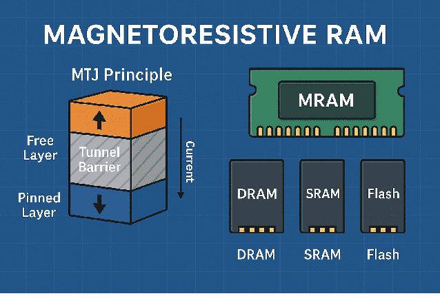
Magnetoresistive Random Access Memory (MRAM) is a non-volatile memory technology. It stores data by leveraging the magnetic orientation of ferromagnetic layers. The traditional memories rely on electric charge (as in DRAM or Flash). MRAM utilizes the spin of electrons. The spin of electrons is a quantum property. That is used to represent binary states.
MRAM stores data using magnetic states rather than electric charges or current flows. The core principle of MRAM is based on magnetoresistance, specifically tunneling magnetoresistance (TMR). It is a quantum mechanical effect observed in a structure known as a Magnetic Tunnel Junction (MTJ).
An MTJ consists of:
- Two ferromagnetic layers are separated by a thin insulating layer (usually magnesium oxide, MgO).
- One ferromagnetic layer has a fixed magnetic orientation (the “reference” layer).
- The other layer’s orientation is free to change (the “free” layer) depending on the bit value.
The resistance of the MTJ depends on the relative orientation of these two layers:
- Parallel alignment (↓ ↓ or ↑ ↑): low resistance = logic 0
- Antiparallel alignment (↑ ↓ or ↓ ↑): high resistance = logic 1
This resistance difference is due to the Tunneling Magnetoresistance (TMR) effect. At TMR electron tunneling probability varies with magnetic alignment. That allows for data readout without altering the stored information.
This magnetic state is retained even when power is removed. That is making MRAM inherently non-volatile. Furthermore, MRAM supports bit-level random access. Bit-level random access allows MRAM for fast read and write operations comparable to SRAM and DRAM but without data loss on power-down.
Magnetoresistive Random Access Memory (MRAM) Key Characteristics:
- Non-volatility: Data is retained even when power is removed.
- Fast switching: Comparable to SRAM and DRAM in access times.
- High endurance: Can withstand >10¹⁵ read/write cycles.
- Radiation hardening: Inherently resistant to cosmic rays and soft errors. That makes it suitable for space and defense applications.
Origin and Evolution of MRAM
The conceptual foundation of MRAM lies at the intersection of magnetism, materials science, and quantum mechanics, particularly in the field known as spintronics (spin-based electronics).
The concept of magnetic memory began with magnetic-core memory. That was used in early mainframe computers. While conceptually similar, it was bulky and manually wired.
Early Research (1960s–1980s)
The first mention of magnetoresistive effects in materials like permalloy occurred in the 1960s.
In 1975, Julliere demonstrated magnetoresistance in tunnel junctions, proposing a model for spin-polarized tunneling. It is a precursor to MTJs.
In the 1980s, Giant Magnetoresistance (GMR) was discovered independently by Albert Fert and Peter Grünberg—work that earned them the 2007 Nobel Prize in Physics.
GMR and the related Tunnel Magnetoresistance (TMR) effect became foundational phenomena enabling practical magnetic memory.
The Birth of MRAM (1990s)
- The first experimental MRAM cells were developed in the mid-1990s by companies like IBM, Honeywell, and Motorola.
- By 1996, Motorola (later Freescale Semiconductor) introduced the first commercial MRAM product in 2006, though it was based on the Toggle MRAM design with limited density and scalability.
Modern MRAM (2010s–present)
- The development of Spin-Transfer Torque (STT) and later Spin-Orbit Torque (SOT) mechanisms dramatically improved MRAM’s scalability and performance. STT allows current-induced magnetization switching without external magnetic fields.
- Companies like Everspin Technologies, Samsung, TSMC, and GlobalFoundries began integrating MRAM into embedded systems and system-on-chip (SoC) platforms.
- By 2018–2022, MRAM started seeing real commercial deployment in microcontrollers, FPGAs, aerospace systems, and enterprise-grade storage systems.
Present and Future
- MRAM is now viewed as a contender for universal memory. This is the single technology that can replace both volatile and non-volatile memory.
- Next-gen MRAM (SOT-MRAM) offers sub-nanosecond switching and extreme endurance. That is suitable for AI accelerators, in-memory computing, and neuromorphic systems.
Today, MRAM is positioned as a candidate for universal memory. It is employed with applications spanning from cache-level memory to non-volatile storage, and on-chip memory in AI accelerators.
Types of Magnetoresistive Random Access Memory (MRAM) and Their Differences
Over the years, several variants of MRAM have been developed. However, each one is addressing specific performance, density, and power requirements.
The major types include:
-
Toggle MRAM
Technology Overview
- Uses magnetic fields generated by current-carrying lines to switch the magnetic orientation of the free layer.
- Based on Amperian field switching.
- First-generation MRAM technology.
Characteristics
- Robust and mature
- Write operations are power-intensive due to the need to generate magnetic fields.
- Susceptible to disturbances in adjacent cells (write selectivity issues)
Use Case
- Suitable for aerospace, military, and industrial applications requiring radiation-hard, deterministic non-volatile memory
Advantages:
-
- Mature and well-understood.
- High reliability and deterministic switching.
Disadvantages:
-
- Requires relatively high power due to current lines.
- Cross-talk and write disturbance limit scalability.
-
STT-MRAM (Spin-Transfer Torque MRAM)
Technology Overview
- Replaces magnetic field switching with spin-polarized current injection.
- The spin torque exerted by electrons flips the magnetic orientation of the free layer.
- Eliminate the need for external magnetic fields.
Characteristics
- Scalable and energy-efficient compared to Toggle MRAM
- A higher density allows integration into embedded applications
- Write latency is higher than DRAM. However, it is acceptable for many applications
- Endurance: >10¹⁵ cycles in optimized configurations
Use Case
- Used in embedded memory for microcontrollers and SoCs
- Increasingly considered for last-level caches (LLC) in CPUs and GPUs
- Found in products by Samsung (embedded STT-MRAM), TSMC, and GlobalFoundries
- Used as last-level caches in CPUs and GPUs.
-
- Low power consumption.
- Highly scalable to sub-20nm nodes.
- Compatible with CMOS back-end-of-line (BEOL) processes.
Disadvantages:
-
- Still susceptible to write disturbance due to shared read/write paths.
-
SOT-MRAM (Spin-Orbit Torque MRAM)
Technology Overview
- Leverages spin-orbit coupling to generate torque via in-plane current. That is enabling faster and more energy-efficient switching.
- Decouples read and write paths. That is reducing write disturbance and improving reliability.
- Extremely fast switching speeds (sub-nanosecond range)
- Lower write energy compared to STT-MRAM
- More suitable for high-speed caches and real-time logic-in-memory applications
- Still in the early commercial stages
- Achieves sub-nanosecond switching speeds with excellent endurance (>5×10¹⁰ cycles)
Use Case
- Candidate for L1/L2 cache replacement
- Ideal for AI/ML accelerators, in-memory computation, and ultra-low-power edge devices
Advantages:
-
- Decouples read and write paths—improving endurance.
- Supports faster write speeds (<500ps).
- Ideal for high-speed logic-in-memory applications.
Disadvantages:
-
- Fabrication complexity increases.
- Not yet mass adopted but under active development.
-
Thermally Assisted MRAM (TA-MRAM)
- Combines thermal heating with magnetic field or STT to assist in switching
- Used to improve write selectivity in earlier MRAM designs
- Now mostly replaced by STT and SOT MRAM
- Voltage-Controlled MRAM (VC-MRAM) (Experimental)
Principle: Uses voltage pulses to modulate anisotropy or interlayer exchange coupling. That is potentially reducing switching energy to attojoules.
- Potential Advantages:
- Ultra-low-power operation.
- Suitable for batteryless or energy-harvesting devices.
- Current Status:
- Active academic and pre-commercial research phase.
- May become crucial in neuromorphic and sensor-driven computing.
Comparison Summary:
| Type | Switching Mechanism | Speed | Power Efficiency | Maturity | Ideal Use Case |
| Toggle MRAM | Magnetic field | Moderate | Low | Mature (legacy) | Aerospace, defense |
| STT-MRAM | Spin-polarized current | High | Medium | Commercial | Embedded memory, IoT, caches |
| SOT-MRAM | Spin-orbit torque | Very High | High | Emerging | AI accelerators, fast caches |
| TA-MRAM | Thermal + magnetic field | Moderate | Low | Obsolete | Historical only |
Why MRAM Matters: Technological Significance and Differentiation
| Property | MRAM | DRAM | NAND Flash |
| Volatility | Non-volatile | Volatile | Non-volatile |
| Speed | ~10 ns (SOT: <1ns) | ~10–15 ns | ~100 µs–1 ms |
| Endurance | 10¹⁴–10¹⁵ cycles | 10⁸–10⁹ cycles | 10³–10⁵ cycles |
| Radiation Resilience | Excellent | Moderate | Poor |
| Scalability | High (sub-20nm nodes) | Moderate | Excellent |
| Integration | CMOS-compatible | DRAM-specific process | Flash-specific process |
Final Notes on Magnetoresistive Random Access Memory (MRAM)’s Typology
Each variant of MRAM has evolved to address the Scalability–Speed–Power triangle. That is aiming to meet different demands. It is employed in various industries, like mission-critical aerospace systems and on-chip machine-learning inference engines. As fabrication techniques mature, magnetic materials improve, and integrated spintronic logic emerges, MRAM types like STT and SOT are increasingly being viewed not only as memory but as computational enablers.
Detailed Physical Principles Behind MRAM Switching
Spin-Dependent Tunneling
At the heart of MRAM’s operation lies the quantum mechanical phenomenon known as spin-dependent tunneling through an insulating barrier:
- In a Magnetic Tunnel Junction (MTJ), electrons maintain their spin polarization as they tunnel through a thin MgO barrier.
- The probability of tunneling depends on whether the spin of the electron matches the magnetic orientation of the destination layer.
- This leads to the Tunneling Magnetoresistance (TMR) effect. In it, the resistance difference between parallel and antiparallel states is measurable and used to store binary information.
Spin-Transfer Torque (STT) Switching
- A spin-polarized current exerts a torque on the free layer. That is inducing a precession that can flip its magnetization.
- Critical switching parameters:
- Spin polarization (P) of the current source
- Gilbert damping (α) of the magnetic layer
- Thermal stability factor (Δ) which ensures non-volatility
- STT is current-driven. It requires careful current pulse engineering to minimize the write error rate while ensuring deterministic switching.
Spin-Orbit Torque (SOT) Switching
- In SOT-MRAM, the in-plane current is passed through a heavy metal with strong spin-orbit coupling (W, Pt).
- This generates a transverse spin current via the Spin Hall Effect.
- The spin current enters the magnetic layer and induces switching via damping-like torque. Those are decoupling the read and write paths.
- This allows for:
- Faster write speed (<1 ns)
- Higher endurance (>10¹⁶ cycles)
- Reduced read-disturb risk
Materials Used in MRAM
2.1 Magnetic Layers
- CoFeB (Cobalt Iron Boron) is the most widely used material for free and reference layers due to:
- High spin polarization
- Good amorphous structure when deposited
- Compatibility with MgO barriers for high TMR
2.2 Tunnel Barrier
- Magnesium Oxide (MgO):
- Acts as the tunneling barrier
- Provides coherent tunneling through Δ1 symmetry states
- Enables TMR ratios exceeding 200%
2.3 Heavy Metal Layers in SOT-MRAM
- Tungsten (W), Tantalum (Ta), Platinum (Pt):
- Chosen for large spin Hall angle
- Must exhibit good thermal and chemical stability
- Critical for spin-orbit torque efficiency
2.4 Pinning Layers
- Antiferromagnetic materials like IrMn or PtMn are used to fix the reference layer’s magnetization direction via exchange bias.
Fabrication and Integration Challenges
3.1 Thermal Budget
- MRAM must be fabricated at temperatures below 400°C to preserve MgO barrier integrity and prevent interdiffusion.
- This necessitates BEOL (Back-End-of-Line) integration after logic transistors are formed.
3.2 Lithographic Alignment
- MTJ stacks require precision patterning to define elliptical nanopillars (down to ~20 nm).
- Misalignment can degrade switching behavior and TMR.
3.3 Process Variability
- Challenges include:
- Thickness uniformity of MgO (~1 nm)
- Magnetic anisotropy control
- Controlling sidewall oxidation and redeposition during etching steps
3.4 Scalability
- Reducing MTJ size below 20 nm causes:
- Increased switching current density
- Retention degradation (due to smaller volume, lower Δ)
- Advanced solutions:
- Use of synthetic antiferromagnetic coupling
- Dual-MTJ or perpendicular MTJ (pMTJ) configurations
Error Rates, Variability, and Correction Mechanisms
4.1 Write Error Rate (WER)
- WER depends exponentially on the pulse amplitude, width, and Δ.
- Typical acceptable WER < 10⁻⁶ for embedded memory use.
- Trade-off: A larger write pulse improves switching probability. However, it increases power and write disturb risk.
4.2 Read Disturb and Read Error
- Read current can inadvertently induce switching if it approaches the critical switching threshold.
- SOT and dual-MTJ designs help decouple read/write paths to mitigate this.
4.3 Error Correction Techniques
- ECC engines (Hamming, BCH) integrated into the memory controller
- Read-verify-write (RVW) schemes for reliability-critical applications
Trade-offs: Endurance vs Retention vs Performance
| Factor | Influence | Trade-off Example |
| Thermal stability (Δ) | Improves retention | Higher Δ = higher write current needed |
| Write current | Affects speed and endurance | Lower current → slower but longer life |
| Read margin | Impacts reliability | Wider margin = more stable, less dense |
| Anisotropy energy (Keff) | Controls switching behavior | pMTJ provides better scaling but is complex to fabricate |
How Does Magnetoresistive Random Access Memory (MRAM) Work?
Magnetoresistive RAM (MRAM) stores data using magnetic states rather than electric charge or current flow. The fundamental mechanism relies on Spintronics. It is the manipulation of electron spin, combined with quantum tunneling across insulating barriers. MRAM cells operate using magnetic tunnel junctions (MTJs). In which logical bits (0 or 1) are determined by the relative alignment of two ferromagnetic layers.
Magnetic Tunnel Junction (MTJ) Principle
Structure of an MTJ
A typical MTJ is composed of three layers:
- Fixed (reference) ferromagnetic layer — magnetization is pinned in one direction using exchange bias via an antiferromagnet (IrMn).
- Tunnel barrier — a thin insulating layer. It is usually MgO. That allows quantum tunneling.
- Free ferromagnetic layer — magnetization is free to switch between parallel and antiparallel relative to the fixed layer.
Tunneling Magnetoresistance (TMR)
- Parallel alignment → low resistance state (bit = 0)
- Antiparallel alignment → high resistance state (bit = 1)
The TMR ratio is defined as:
TMR = (R_AP – R_P) / R_P
Where:
- R_AP is resistance in an antiparallel state
- R_P is resistance in parallel state
In high-quality MgO-based MTJs, TMR > 200% is common due to coherent tunneling through Δ1 symmetry states in the MgO crystal.
Spintronics Basics
Spin and Magnetization
Electrons possess a quantum mechanical property called spin. The spin can be treated as intrinsic angular momentum. In ferromagnetic materials:
- Electrons align their spins due to exchange interaction.
- This net alignment produces macroscopic magnetization (M).
Spintronics leverages this spin degree of freedom, in contrast to traditional electronics, which only uses charge.
Spin-Transfer Torque (STT)
Discovered in the 1990s, STT allows for magnetization switching without external magnetic fields. Key mechanisms:
- A spin-polarized current is injected through the MTJ.
- Angular momentum transfer from the polarized electrons applies torque on the free layer.
- If the current exceeds the critical switching current (Ic), the free layer flips.
The dynamics of magnetization (M) are described by the Landau-Lifshitz-Gilbert (LLG) equation augmented by a spin torque term:
dM/dt = -γ M x H_eff + α M x dM/dt + τ_STT
Where:
- γ is the gyromagnetic ratio
- α is the Gilbert damping constant
- τ_STT is the spin-transfer torque term
Spin-Orbit Torque (SOT)
A more recent advancement uses spin-orbit coupling in heavy metals:
- Current flows in-plane through a heavy metal like Pt or W.
- Via the spin Hall Effect, a transverse spin current is generated.
- This spin current flows into the magnetic free layer, switching it.
SOT offers:
- Decoupled read/write paths
- Sub-nanosecond switching
- Reduced write energy
Comparison with Other Memory Types
| Feature | MRAM | DRAM | SRAM | Flash |
| Data Storage | Magnetic state | Capacitor charge | Bistable latch | Trapped charge in floating gate |
| Non-volatility | Yes | No | No | Yes |
| Read Speed | ~5 ns | ~10–20 ns | ~1–2 ns | ~50–100 ns |
| Write Speed | 1–10 ns (STT), <1 ns (SOT) | ~10 ns | ~1 ns | ~1 μs (block erase) |
| Endurance | 10^13–10^16 cycles | ~10^8 | >10^16 | 10^3–10^6 cycles |
| Density | Moderate | High | Low | Very high |
| Power Use | Low standby, moderate write | High refresh power | High dynamic | Very low standby |
| Scaling Limits | MTJ scaling <20 nm challenging | Capacitor leakage at small nodes | Cell area (6T) | Tunnel oxide reliability |
| Radiation Hardness | Excellent | Poor | Moderate | Poor |
Key Takeaways for Researchers
- MRAM represents the intersection of quantum mechanics (tunneling), solid-state magnetism (ferromagnetism), and Spintronics (angular momentum transfer).
- The success of MRAM technology hinges on optimizing TMR, spin polarization, damping factors, and switching thresholds.
- Unlike volatile charge-based memories, MRAM offers intrinsic resilience to radiation, soft errors, and power loss. That makes it ideal for aerospace, IoT, edge-AI, and automotive safety systems.
- Research continues in multi-level MRAM, voltage-controlled switching, and 3D stacking, pushing MRAM toward replacing SRAM in the cache or even as a universal memory.
Advantages of Magnetoresistive Random Access Memory (MRAM)
Magnetoresistive Random Access Memory (MRAM) is a cutting-edge non-volatile memory (NVM) technology. MRAM addresses many of the bottlenecks faced by conventional memory architectures. Leveraging the physics of electron spin and magnetic tunnel junctions (MTJs), MRAM delivers a rare confluence of properties like high speed, data retention without power, low energy usage, and robust durability. These features make MRAM technologically superior in many aspects. However, it is also strategically important in emerging computational paradigms.
-
Non-volatility
Fundamentals:
MRAM stores bits using magnetic orientation rather than electric charge. The state of the MTJ namely parallel or antiparallel magnetization remains stable without electrical bias due to magnetic anisotropy barriers.
Physics Insight:
- Magnetic domains remain fixed due to energy minima determined by magnetocrystalline anisotropy and shape anisotropy.
- The energy barrier ΔE between states governs retention time, with ΔE ≫ kT (Boltzmann constant × temperature) ensuring long-term stability.
Implications:
- Zero standby power consumption: No refresh cycles like DRAM.
- Persistent storage: Ideal for mission-critical systems.
- Data resilience: Survives power interruptions, system crashes, and extreme environments.
Emerging Use Cases:
- Power-failure resilient computing
- Secure memory for embedded AI/ML models
- Instant-on systems for edge devices
-
Fast Read/Write Speeds
Mechanisms:
- In STT-MRAM, data is written by passing a spin-polarized current through the MTJ.
- SOT-MRAM allows even faster writes by decoupling read and write paths to mitigate read-disturb issues.
Key Metrics:
- STT-MRAM: ~5–10 ns writes
- SOT-MRAM: <1 ns switching, ideal for cache replacement
Technical Comparison:
- Flash: ~10 µs write latency
- DRAM: ~10–20 ns write latency
- SRAM: ~1–2 ns, but volatile
Physics Basis:
- Based on Landau-Lifshitz-Gilbert-Slonczewski (LLGS) dynamics for magnetization switching.
- Switching delay depends on factors like Gilbert damping (α), spin polarization, and effective anisotropy.
Academic Research Direction:
- Reducing switching time while minimizing the write error rate
- Thermally assisted switching for faster performance at lower current
-
Low Power Consumption
Why It Is Efficient:
- No need for constant refreshing or charge retention (unlike DRAM).
- Current-driven switching consumes energy only during state transitions.
- No leakage in standby: MRAM cells are passive when idle.
Quantitative Example:
| Technology | Active Power per Bit | Standby Power |
| DRAM | ~20–100 pJ | High (refresh) |
| SRAM | ~1–10 pJ | Moderate |
| MRAM | ~0.1–1 pJ | ~0 W (ideal) |
Research Context:
- STT-MRAM switching energy scales with current density and junction area (J × A).
- Voltage-controlled MRAM (VCMA) seeks to reduce write energy <10 fJ per bit.
Applications:
- Battery-powered IoT sensors and medical implants
- Always-on devices (smartwatches)
- Ultra-low-power AI accelerators
-
High Endurance and Longevity
Definition:
Endurance defines how many read-write cycles a memory cell can tolerate before degradation.
Why MRAM Excels:
- No physical movement of atoms or destructive tunneling (as in Flash)
- MTJ switching does not degrade oxide integrity
- Switching is magnetic. Switching is not electrical breakdown-based
Typical Endurance Values:
- Flash: 10³–10⁶ cycles (limited by tunnel oxide damage)
- DRAM: 10⁷–10⁸ cycles (capacitor fatigue)
- MRAM: ≥10¹³ cycles (depending on design)
Scientific Detail:
- Fatigue failure in MRAM is linked to stochastic thermal activation. That is not physical wear.
- Current density optimization reduces electromigration risk in interconnects.
Commercial Implication:
- Suitable for cache, scratchpad, and real-time logs
- Reduces wear-leveling complexity in file systems
- Lower TCO (Total Cost of Ownership) for industrial memory systems
-
Radiation Hardness and Environmental Resilience
Overview:
MRAM is inherently immune to single-event upsets (SEUs) caused by alpha particles, gamma rays, or cosmic radiation. Thanks to its magnetic nature.
Scientific Basis:
- Magnetic states are not disrupted by ionizing radiation
- MTJs do not rely on charge storage vulnerable to high-energy particles
Use Cases:
- Aerospace systems
- Nuclear energy control systems
- Deep space missions
Supporting Research:
- Studies confirm MRAM retains function in >100 krad(Si) environments
- Found in satellites, Mars rovers, and avionics control units
-
Scalability and Integration Potential
Scaling Trends:
- Current MTJ diameters: ~20–50 nm
- Below 20 nm, maintaining TMR and thermal stability is challenging
Research Areas:
- Advanced patterning (EUV lithography, self-aligned etch)
- Perpendicular Magnetic Anisotropy (PMA) for smaller, stable cells
- VCMA and SOT to reduce power while enabling high-speed switching
Integration Potential:
- Compatible with CMOS BEOL (Back-End-of-Line) processing
- Foundry support: TSMC, Samsung, and GlobalFoundries have added MRAM to advanced nodes (28nm, 22nm, 16nm FinFET)
-
Application Versatility
MRAM can replace or complement several existing memory types:
| Use Case | Replaces | Benefit |
| Embedded non-volatile | Flash, EEPROM | Faster, more durable |
| SRAM cache | SRAM | Lower leakage, non-volatility |
| DRAM replacement | DRAM (partial) | No refresh, lower standby power |
| AI inference buffers | SRAM, DRAM | Speed and persistence combined |
| Harsh environments | Flash, DRAM | Radiation tolerance |
Comparative Benchmarking: MRAM vs. ReRAM, PCM, and FeRAM
| Feature | MRAM | ReRAM | PCM | FeRAM |
| Cell Structure | Magnetic Tunnel Junction (MTJ) | Metal–Insulator–Metal (MIM) | Chalcogenide phase-change stack | Ferroelectric capacitor |
| Switching Mechanism | Spin-transfer or spin-orbit torque | Filament formation/rupture | Crystalline ↔ Amorphous states | Ferroelectric polarization |
| Write Energy | ~0.1–1 pJ/bit (STT)
<10 fJ (VCMA) |
~1–10 pJ/bit | ~1–10 pJ/bit | ~0.1–1 pJ/bit |
| Read Latency | ~5–30 ns | ~10–100 ns | ~50–100 ns | ~20–100 ns |
| Write Latency | ~5–50 ns (STT)
~1 ns (SOT) |
~10–100 ns | ~100–1000 ns | ~50–100 ns |
| Endurance | >10¹³ cycles (SOT/STT) | ~10⁸–10¹² cycles | ~10⁷–10⁹ cycles | ~10¹⁰–10¹⁵ cycles |
| Retention | >10 years @ 85°C | >10 years | >10 years | ~10 years |
| Scalability | ~20 nm (lab), 22–28 nm (prod) | Scales to sub-10 nm | ~20 nm | Difficult <28 nm |
| CMOS Compatibility | BEOL compatible | BEOL compatible | Mid to BEOL, thermally sensitive | Challenging integration |
| Radiation Hardness | Excellent | Good | Moderate | Moderate |
| Maturity / Commercial Use | Available @ 22nm (e.g., GF, Samsung) | Prototype level
Some niche products |
Intel Optane (now discontinued), enterprise NVDIMMs | Available in some MCUs (TI, Fujitsu) |
| Key Applications | Cache, storage-class memory, embedded NVM, AI edge | NVM for IoT, neuromorphic computing | Storage-class memory, in-memory computing | Low-power MCUs, RFID, smartcards |
Comparative Technical Analysis
-
Endurance and Reliability
- MRAM and FeRAM exhibit the highest endurance. They are suitable for frequent write operations like in caches, metadata logs, and real-time analytics.
- PCM and ReRAM degrades with cycling due to filament fatigue (ReRAM) or phase wear-out (PCM). That is making them better for archival or read-dominant tasks.
-
Write Energy and Speed
- VCMA-MRAM and FeRAM lead in energy efficiency (~femtojoule levels), ideal for ultra-low-power systems.
- PCM comes with thermal switching. PCM is slower and more power-hungry. In addition, it needs Joule heating to alter phase states.
- ReRAM varies: newer materials like HfOx improve energy profile. However, its variability is still a concern.
-
Latency
- MRAM matches or even surpasses SRAM in read/write latency with SOT variants.
- FeRAM also provides fast switching due to polarization-based write. That makes it attractive for real-time control systems.
- PCM and ReRAM are slower due to thermal and stochastic effects respectively.
-
Scalability
- ReRAM is the most scalable (sub-10 nm nodes). It is aided by simple 1T1R or crossbar architectures.
- MRAM is scalable to 20 nm with PMA MTJs. However, its challenges include maintaining TMR (tunnel magnetoresistance) and write error rates at small dimensions.
- FeRAM faces difficulty scaling due to the need for ferroelectric capacitors and their volatile polarization behavior at sub-20 nm.
-
Integration with CMOS and Fabrication
- MRAM and ReRAM are the most CMOS-friendly and are already being integrated at advanced nodes (TSMC and GF 22FDX with eMRAM).
- PCM poses challenges due to high-temperature annealing and materials (GeSbTe) not native to CMOS flows.
- FeRAM faces integration barriers due to ferroelectric layer deposition and materials compatibility.
-
Radiation Tolerance
- MRAM stands out due to magnetic switching rather than charge movement. It is ideal for space, nuclear, and defense applications.
- ReRAM has good radiation hardness depending on materials.
- PCM and FeRAM are moderately susceptible to single-event effects due to their charge-based nature.
Choosing the Right Memory: Application Matrix
| Application Domain | Preferred Memory |
| Embedded MCUs / IoT | MRAM, FeRAM |
| Automotive Safety Systems | MRAM |
| AI Edge Accelerators | MRAM, ReRAM |
| Data Center Storage Tiering | PCM |
| Space Systems / Radiation Zones | MRAM |
| Wearables / Medical Implants | FeRAM, MRAM |
| Neuromorphic Computing | ReRAM, PCM |
Research & Development Outlook
- MRAM: SOT-MRAM and VCMA-MRAM offer sub-nanosecond switching and ultra-low energy. It is ideal for future cache and logic-in-memory integration.
- ReRAM: Research in analog switching, stochastic computing, and synaptic weights supports neuromorphic systems.
- PCM: Despite commercial retreat, it remains promising in in-memory computing and computational storage.
- FeRAM: With HfZrO-based ferroelectrics. Researchers are exploring scalable FeFETs as logic-compatible memory alternatives.
Challenges and Limitations of MRAM
Magnetoresistive RAM (MRAM) holds immense promise as a next-generation memory technology. However, its adoption at scale is not without significant technical, physical, and economic challenges. Understanding these constraints is essential for system designers, materials scientists, and semiconductor engineers, those who are aiming to integrate MRAM into practical computing architectures.
-
Scaling Limitations of Magnetic Tunnel Junctions (MTJs)
Issue:
As MRAM scales to sub-20 nm nodes, several quantum and material limitations begin to impact performance and stability.
Detailed Explanation:
- Thermal Stability Factor (Δ = E/kT) decreases with reduced MTJ volume. That is threatening data retention. A smaller MTJ area means a lower magnetic anisotropy energy barrier. That lower magnetic anisotropy energy barrier is increasing the risk of spontaneous bit flips.
- Maintaining high Tunnel Magnetoresistance (TMR) becomes more difficult at the nanoscale. That is reducing the read signal margin and increasing bit error rates.
- Variability in MTJ resistance-area (RA) products and magnetic anisotropy leads to inconsistency in device performance.
Ongoing Research:
- Use of materials with high perpendicular magnetic anisotropy (PMA) like CoFeB/MgO interfaces.
- Shape engineering of free layers to maintain energy barriers while reducing lateral footprint.
-
High Write Current Requirements (STT-MRAM)
Issue:
Spin-transfer torque (STT) MRAM requires high current densities (~10⁶–10⁷ A/cm²) for switching. That is leading to increased power consumption and design complexity.
Implications:
- Elevated power during write operations can cause electromigration and self-heating. That is potentially damaging the MTJ stack.
- Difficult to share with logic transistors in scaled CMOS processes.
- A trade-off exists between write speed, energy, and retention. The faster writes demand more current. That shortens lifetime and raises energy usage.
Mitigation Strategies:
- Spin-Orbit Torque (SOT) MRAM decouples read/write paths and reduces required current.
- Voltage-Controlled Magnetic Anisotropy (VCMA) MRAM can reduce switching energy below 1 fJ per bit. However, it is still largely in the R&D phase.
-
Write Error Rate (WER) and Reliability Concerns
Issue:
The inherently stochastic nature of magnetization switching. That is more particularly true in STT and VCMA mechanisms. It leads to write failure probabilities.
Details:
- Write Error Rate (WER) depends exponentially on the write pulse width and current.
- Environmental noise (thermal, EMI), process variation, and MTJ variability can worsen WER.
- For mission-critical systems, uncorrected WER >10⁻⁹ is unacceptable.
Solutions:
- Use of error correction codes (ECC) and redundancy in high-reliability applications.
- Improved MTJ stack design with materials that have sharp switching distributions.
-
Material Integration and Fabrication Complexity
Issue:
MRAM fabrication involves specialized magnetic materials and ultra-thin oxide layers (MgO). Those are not standard in CMOS logic fabs.
Key Challenges:
- Integration of magnetic stacks into CMOS Back-End-of-Line (BEOL) without degrading thermal or electronic characteristics.
- Avoiding cross-talk and magnetic coupling between adjacent bits.
- MTJ patterning at the nanoscale requires precise etch control to avoid damage to the tunnel barrier.
Foundry Status:
- Available at 22–28 nm nodes (GlobalFoundries, Samsung, TSMC). However, there is limited support at <14 nm.
- VCMA and SOT layers may introduce material contamination risks in advanced CMOS nodes.
-
Cost and Density Limitations
Issue:
MRAM has not yet achieved the bit density or low cost per gigabyte required to replace DRAM or Flash at scale.
Reasons:
- 1T1MTJ structure: Requires a dedicated access transistor. That is limiting areal density.
- Difficult to implement in 3D stacking architectures (unlike NAND Flash).
- Lower economies of scale due to limited production volume and fab adoption.
Possible Workarounds:
- Use MRAM in hybrid architectures (DRAM + MRAM, SRAM + MRAM).
- Research into multi-level cell (MLC) MRAM, although error margins are currently high.
-
Read Disturb and Sneak Paths
Issue:
In high-density crossbar arrays (especially with STT-MRAM), read and write operations can inadvertently disturb adjacent cells.
Details:
- Magnetic field fringing and leakage currents can cause read-disturb errors.
- Crossbar arrays suffer from sneak current paths. That is reduce selectivity and increase noise.
Solutions:
- Use of access transistors (1T1MTJ) or selection devices (selector diodes).
- Transitioning to SOT-MRAM helps isolate read and write paths more effectively.
-
Temperature and Magnetic Field Sensitivity
Issue:
MRAM has good high-temperature retention. Its magnetic memory is naturally sensitive to ambient magnetic fields.
Risks:
- External magnetic fields (from nearby electronics) can flip bits or degrade read/write fidelity.
- Local heating from high write currents may impact nearby logic circuits in System-on-Chip (SoC) designs.
Mitigation:
- Use of shielding layers in chip packaging.
- Employing antiferromagnetically coupled layers to stabilize the free layer.
Summary: MRAM Challenge Matrix
| Challenge | Impact Area | Current Status |
| MTJ scaling limits | Density, retention | Active materials research ongoing |
| High write currents | Power, endurance | SOT/VCMA being developed |
| Write error rate (WER) | Reliability | ECC + better MTJ stack engineering |
| Fabrication complexity | Yield, cost | BEOL compatible at mature nodes (22–28nm) |
| Cost per bit | Commercial viability | Still higher than DRAM/Flash |
| Magnetic interference | System integrity | Shielding and stack design under research |
| Crossbar sneak paths | Architecture scaling | Selector devices and design optimization |
Outlook: Can MRAM Overcome These Challenges?
Despite these limitations, MRAM continues to evolve rapidly:
- SOT-MRAM is being evaluated as a replacement for SRAM caches.
- Voltage-driven switching (VCMA) is reducing write energy towards sub-femtojoule levels.
- CMOS-compatible MTJ stacks and integration into foundry PDKs make MRAM a prime candidate for in-logic non-volatility.
The technology may not replace DRAM or Flash outright in the next 2–3 years. However, its niche dominance in:
- Radiation-hardened environments,
- Edge AI accelerators,
- Always-on devices,
- Automotive safety systems,
MRAM will play a crucial role in future heterogeneous memory hierarchies.
Applications of Magnetoresistive Random Access Memory (MRAM)
Magnetoresistive Random Access Memory (MRAM), with its combination of non-volatility, high speed, low power, and excellent endurance, has found a growing number of use cases across the computing landscape. As manufacturing matures and spintronic innovation accelerates, MRAM is being adopted in commercial products ranging from embedded systems to AI edge devices.
This section explores the key application domains of MRAM. Let us delve into the architectural motivations and performance trade-offs in each context.
-
Embedded Systems and Microcontrollers (MCUs)
Why MRAM?
- Replaces embedded Flash and SRAM in microcontrollers with non-volatility and instant-on behavior.
- Offers a simplified memory hierarchy by serving as both program memory and data storage.
Real-World Implementations:
- NXP i.MX RT500/600 series: Combines Cortex-M cores with embedded MRAM. It is targeting ultra-low-power IoT and wearables.
- TSMC and GlobalFoundries support MRAM IP for SoCs at 22nm nodes.
Use Cases:
- Wearables
- Smart meters
- Consumer electronics
- Secure microcontrollers (with tamper resistance)
-
Industrial and Automotive Electronics
Why MRAM?
- Endurance (>10¹² cycles) and radiation tolerance make MRAM suitable for safety-critical and rugged environments.
- No need for periodic refreshes. That improves system reliability and reduces energy budgets.
Functional Benefits:
- Instant-on boot enables rapid startup times for ADAS (Advanced Driver Assistance Systems).
- Error resistance is critical in high EMI environments like electric vehicles or factory automation.
Standards and Usage:
- MRAM has passed the AEC-Q100 automotive-grade qualification in several SoC families.
- Used in black box recorders, infotainment systems, and real-time control.
-
AI Edge Computing and Inference Accelerators
Why MRAM?
- Fast random access and read endurance (>10¹⁵ cycles) support parameter loading and weight storage in inference engines.
- Non-volatility allows state preservation across power cycles. It enables more efficient always-on applications.
Architectural Roles:
- Store neural network weights in-memory. It is reducing DRAM access.
- Use in ReRAM-MRAM hybrids for combining analog training with digital inference.
Use Cases:
- TinyML (Tiny Machine Learning) devices
- Edge AI accelerators in cameras, drones, and smart sensors
- Always-on voice and face recognition modules
-
Storage Class Memory (SCM) and NVDIMMs
Why MRAM?
- High endurance and fast writes make MRAM suitable for bridging the latency gap between DRAM and Flash in SCM use cases.
- Can be used to build persistent caches, journaling layers, or transaction logs in storage systems.
Performance Fit:
- Lower latency and higher endurance than NAND Flash
- Better reliability and lower write amplification than PCM
Industry Developments:
- Everspin offers MRAM-based SSDs and NVDIMMs.
- Interest from enterprise storage vendors for use in metadata caching and journaling.
-
Aerospace and Defense
Why MRAM?
- Radiation hardening and immunity to single-event upsets (SEUs) due to magnetic switching make MRAM ideal for space systems and military electronics.
- Retains data through power loss, vibration, and temperature extremes.
Applications:
- Satellite data recorders
- Tactical radios and radar systems
- Secure mission data logging (no bootup loss)
Proven Systems:
- NASA and ESA satellite subsystems have employed MRAM for high-reliability non-volatile storage.
-
CPU and GPU Caches (Research & Prototypes)
Why MRAM?
- SOT-MRAM and VCMA-MRAM offer speeds approaching SRAM with zero leakage power. That makes them attractive for L1/L2 cache replacement.
- Enables non-volatile processor states. That is useful for energy harvesting systems or crash-resilient computing.
Challenges:
- Write latency and switching variability must be further reduced.
- Integration with logic at advanced nodes is still in the pilot stage.
Potential Benefits:
- Instant recovery from a system crash or power loss
- Energy savings via cache power gating without data loss
-
Neuromorphic and In-Memory Computing (R&D Phase)
Why MRAM?
- Emerging use of analog MRAM and probabilistic switching for mimicking synaptic behavior.
- Supports non-Boolean computing models and probabilistic AI.
Research Directions:
- Stochastic MRAM: Used for hardware-based Monte Carlo sampling and Boltzmann machines.
- Hybrid MRAM-CMOS arrays: Enable local processing. That is reducing von Neumann bottlenecks.
Use Cases (Under Exploration):
- Brain-inspired computing platforms
- Hardware-accelerated AI training (spiking neural networks)
-
Security-Critical Devices
Why MRAM?
- MRAM’s instant wipe capability (magnetic field or current pulse) can be used to build tamper-resistant memory.
- Non-volatility avoids leaks during power transitions.
Examples:
- Secure cryptographic key storage
- Anti-tamper defense applications
- Digital rights management in content protection
Summary: Application Matrix
| Domain | Use Case | MRAM Feature Exploited |
| Embedded Systems | MCU code/data memory | Non-volatility, endurance |
| Automotive | ECU, infotainment, ADAS | Reliability, instant-on |
| AI Edge Devices | Model storage, parameter memory | Speed, non-volatility |
| Storage Devices | Metadata journaling, caching | Endurance fast writes |
| Aerospace/Defense | Flight logs, secure memory | Radiation hardness, ruggedness |
| Processors (R&D) | L1/L2 cache, context retention | Low leakage, speed |
| Neuromorphic Systems | Probabilistic computing, synapses | Stochastic switching |
| Secure Systems | Tamper-proof memory, key vaults | Wipe capability, data persistence |
MRAM in the Memory Hierarchy
Traditional Memory Hierarchy: A Quick Overview
In modern computer architecture, memory is structured hierarchically. That is prioritizing speed, cost, capacity, and volatility.
Here is how the typical hierarchy looks, from fastest (and most expensive) to slowest (and cheapest):
┌──────────────────────────────────┐
│ CPU Registers (few KB, ns)│ ← Fastest, smallest
├──────────────────────────────────┤
│ L1/L2/L3 Caches (SRAM) │
├──────────────────────────────────┤
│ Main Memory (DRAM) │
├──────────────────────────────────┤
│ Storage (NAND Flash, SSD) │
├──────────────────────────────────┤
│ Magnetic Disks (HDD) │ ← Slowest, largest
└──────────────────────────────────┘
Each layer balances:
- Latency (access time in ns–ms)
- Bandwidth (data throughput)
- Persistence (volatile vs. non-volatile)
- Cost per bit
Where Does MRAM Fit?
MRAM introduces a non-volatile, fast, and high-endurance alternative. It challenges traditional boundaries between working memory and storage.
Depending on the type, MRAM can function at multiple levels of the memory hierarchy:
| MRAM Type | Closest Equivalent | Typical Role | Latency | Volatility | Use Case |
| STT-MRAM | SRAM | Cache, register-level buffers | ~10 ns | No | L1/L2 Cache in low-power CPUs |
| SOT-MRAM | SRAM/DRAM hybrid | High-speed embedded RAM | <5–10 ns | No | AI edge accelerators |
| Embedded MRAM | DRAM | Main memory in MCUs | ~30–50 ns | No | Automotive, industrial IoT |
| Discrete MRAM | Flash | Storage alternative or NVRAM | ~100 ns | No | RAID controllers, boot memory |
Key Insight: Unlike DRAM or Flash, MRAM can collapse two or more layers into one, offering:
- SRAM-like speeds
- DRAM-like endurance
- Flash-like persistence
Hybrid Memory Architectures with MRAM
In real-world deployments, MRAM is increasingly being used in hybrid memory systems, Like:
- eMRAM (Embedded MRAM):
- Integrated into SoCs (System-on-Chip) as cache or working memory
- Replacing embedded Flash in advanced MCUs (in 28nm–22nm nodes)
- MRAM + DRAM Systems:
- MRAM used as a persistent DRAM backup or low-power buffer
- Reduces DRAM refresh energy and improves boot time
- MRAM + NAND Flash Storage:
- MRAM used for fast metadata storage or caching
- Improves SSD performance and reliability
- Unified Memory Architectures (future vision):
- Replace DRAM + Flash with a single MRAM layer
- Enables instant-on computing and persistent working memory
MRAM’s Unique Contribution
MRAM is particularly compelling because it challenges the traditional assumptions of memory hierarchy:
| Feature | Traditional Memory | MRAM Contribution |
| Volatility | DRAM, SRAM (volatile) | MRAM is non-volatile |
| Speed | SRAM (fast), Flash (slow) | MRAM is fast and persistent |
| Endurance | Flash wears out | MRAM has DRAM-like endurance |
| Integration Complexity | Flash is off-chip | MRAM can be embedded on-die |
| Boot-up Times | DRAM refresh required | MRAM enables instant-on systems |
Visual Representation
Here’s an updated memory hierarchy diagram with MRAM included:
┌────────────────────────────────────┐
│ CPU Registers │ ← Fastest, volatile
├────────────────────────────────────┤
│ L1/L2/L3 Caches (SRAM, SOT-MRAM) │
├────────────────────────────────────┤
│ Main Memory (DRAM, STT-MRAM) │
├────────────────────────────────────┤
│ Non-volatile Cache (eMRAM) │
├────────────────────────────────────┤
│ Storage (NAND Flash, MRAM SSDs) │
└────────────────────────────────────┘
MRAM does not fit into a single tier of the memory hierarchy. However, it reshapes the structure entirely. Its flexibility enables:
- Faster, more energy-efficient devices
- Persistent memory closer to the CPU
- Simplified system design with fewer memory layers
This versatility is why MRAM is being studied not just as an alternative, but as a cornerstone of next-generation memory architectures.
Embedded MRAM vs. Standalone MRAM
Understanding the Context
Magnetoresistive RAM (MRAM) can be deployed in two fundamentally different configurations depending on the application’s integration needs, performance requirements, and system design constraints:
- Embedded MRAM (eMRAM): Integrated directly into a System-on-Chip (SoC) or microcontroller (MCU) die.
- Standalone MRAM: Packaged separately as a discrete memory chip and connected to the system via a bus (SPI, DDR, PCIe).
These two implementations serve different roles in computing ecosystems and have unique technical profiles.
Embedded MRAM (eMRAM)
Definition: eMRAM is MRAM technology embedded directly into the same die or process node as logic circuits (CPU, DSP, MCU, etc.).
Characteristics
| Feature | Embedded MRAM |
| Density | Typically low to moderate (kilobytes to few megabytes) |
| Integration | Monolithically integrated with CMOS logic |
| Latency | Ultra-low (few ns), similar to SRAM |
| Power Consumption | Very low; no standby leakage |
| Cost | Higher per-bit cost. However, saved system costs due to integration |
| Process Compatibility | Fully CMOS-compatible (22nm FD-SOI) |
Industry Adoption
- GlobalFoundries offers eMRAM as part of its 22FDX platform.
- Samsung integrated eMRAM into its 28nm FD-SOI technology.
- TSMC has begun offering eMRAM for automotive and IoT MCUs.
Use Cases
- Automotive: Real-time control and instant-on systems
- Industrial IoT: Secure firmware storage, persistent configuration
- Wearables & Edge AI: TinyML models and logs with minimal energy
Standalone MRAM
Definition: MRAM is fabricated as a discrete memory chip. It is housed in its own package and interfaced externally with a processor.
Characteristics
| Feature | Standalone MRAM |
| Density | Moderate to high (megabytes to tens of MB) |
| Integration | External; mounted on board |
| Latency | Higher than embedded, typically 20–50 ns |
| Power Consumption | Higher idle power; still better than Flash |
| Cost | More cost-effective per bit in larger capacities |
| Interface | SPI, DDR, QSPI, parallel NOR-compatible |
Industry Adoption
- Everspin Technologies is the leader in discrete MRAM products.
- MRAM-based DDR3/DDR4-compatible modules are available for servers and RAID controllers.
- Used in space-grade applications due to radiation hardness.
Use Cases
- Storage Controllers: Persistent metadata caching
- RAID Systems: Write journaling and fast recovery
- Aerospace & Defense: Radiation-tolerant data retention
- Consumer Electronics: Boot code, secure storage
Side-by-Side Comparison
| Feature | Embedded MRAM (eMRAM) | Standalone MRAM |
| Form Factor | On-chip (SoC/MCU integration) | External chip/module |
| Density | 256 KB – 8 MB | 4 MB – 64 MB |
| Power Efficiency | Optimized for ultra-low power | Moderate (still better than Flash) |
| Latency | 3–10 ns | 20–50 ns |
| Use Cases | IoT, automotive, wearables | Storage, RAID, space systems |
| Vendors | TSMC, Samsung, GlobalFoundries | Everspin, Avalanche, NVE |
Strategic Implications
- Embedded MRAM is poised to replace embedded Flash, in advanced process nodes (<28nm) where Flash integration is no longer feasible.
- Standalone MRAM serves niche but growing markets like edge analytics, space missions, and ultra-reliable computing.
Both embedded and standalone MRAM offer distinct advantages depending on system needs:
- Use eMRAM when you need fast, integrated, non-volatile memory on the same die as logic, for real-time, low-power applications.
- Use standalone MRAM when you need higher capacity, reliability, and retention in discrete systems, for storage-class or resilient designs.
Their complementary roles are fueling MRAM’s expansion into multiple computing layers, from microcontrollers to storage engines and beyond.
Magnetoresistive Random Access Memory (MRAM) Research Frontiers: Neuromorphic, In-Memory Compute, and Probabilistic Memory
Magnetoresistive RAM (MRAM) is already being adopted in commercial embedded systems and edge devices. However, its true disruptive potential lies at the cutting edge of computer architecture and brain-inspired systems. Researchers are leveraging the physics of spintronics and the stochastic behavior of nanoscale magnetic devices, to explore MRAM for neuromorphic computing, in-memory processing, and probabilistic hardware models.
This section delves into the state-of-the-art research frontiers where MRAM is being reimagined not as a memory, but as a computational primitive.
-
MRAM in Neuromorphic Computing
Motivation:
Neuromorphic systems aim to mimic the neurobiological architecture of the human brain. Neuromorphic systems require devices that behave like neurons and synapses. MRAM provides components with memory and dynamic response of Neuromorphic systems. MRAM, particularly spintronic variants, offers non-volatility, multi-level resistance states, and energy-efficient switching. That makes it a candidate for artificial synapses and neurons.
Research Highlights:
- The stochastic Switching Behavior of MRAM mimics the noisy nature of synaptic transmission. This is useful in implementing biologically plausible learning mechanisms like Spike-Timing Dependent Plasticity (STDP).
- Analog MRAM cells can store weights in a continuous manner. It uses current-controlled partial magnetization. It is a requirement for analog vector-matrix multiplications.
- MRAM-based Leaky Integrate-and-Fire (LIF) neurons have been demonstrated using the dynamic magnetization properties of nanomagnets.
Key Advantages:
- CMOS compatibility for integration into standard silicon neuromorphic chips.
- Long retention time and high endurance support learning over time without loss of state.
- Low standby power for always-on-edge neuromorphic systems.
-
In-Memory Computing with MRAM
Motivation:
The von Neumann bottleneck is the separation of memory and computation. That results in massive energy and latency costs for data movement. In-memory computing (IMC) aims to co-locate computation within or near the memory arrays. MRAM enables this due to its two-terminal structure, non-destructive read, and resistive switching characteristics.
MRAM-Based IMC Techniques:
- Bitwise logic operations: NAND, NOR, and XOR can be performed directly on MRAM arrays using current pulses. That is leveraging magnetoresistive behavior.
- Arithmetic operations: Using MRAM crossbars to execute multiply-accumulate (MAC) operations. That is essential for neural networks and signal processing.
- Matrix-vector multiplication (MVM): Analog-domain in-memory multiply using arrays of MRAM elements with programmable resistance (multi-level cells).
Key Research Projects:
- Integration of STT-MRAM with Processing-in-Memory (PIM) architectures for AI workloads.
- Hybrid systems combine SRAM/DRAM for temporary data and MRAM for parameter memory and compute logic.
- Proposals for MRAM accelerators in edge-AI platforms with 10×–100× reduction in energy compared to DRAM-based solutions.
Challenges:
- Precise control of magnetization for analog computing is difficult due to stochasticity.
- Error accumulation in MAC operations without sufficient precision.
-
Probabilistic and Stochastic Memory Architectures
Motivation:
Traditional digital computation is deterministic. However, many machine learning and optimization problems benefit from stochastic sampling, randomness, and probabilistic modeling. These are the tasks that are expensive on conventional hardware. MRAM’s inherent stochastic switching under near-threshold current can be used to generate randomness in hardware.
Applications:
- Bayesian Neural Networks: MRAM devices are used to generate samples from weight distributions instead of fixed weights.
- Boltzmann Machines and Markov Chain Monte Carlo (MCMC) samplers: Leverage random switching to sample from energy landscapes.
- Probabilistic Bits (p-bits): MRAM-like devices that fluctuate between binary states and can be used to solve NP-hard problems (SAT, Ising models).
Key Concepts:
- By biasing MRAM near its switching threshold, it acts as a hardware random number generator (RNG) or a tunable probabilistic switch.
- Arrays of such devices can be coupled to represent energy-based models and execute parallel stochastic searches.
Experimental Work:
- IBM, Purdue University, and Stanford have published work on p-bit networks using MRAM-like devices.
- Simulated annealing and Ising solvers using low-barrier nanomagnets that switch with thermally-induced randomness.
Materials and Physics Driving These Frontiers
- Low-barrier magnets: Tailored for thermal fluctuation behavior in probabilistic computing.
- Voltage-Controlled MRAM (VCMA): Enables energy-efficient and fine-grained switching for analog computing.
- Synthetic antiferromagnets (SAF): Improve stability and control of MRAM cells in large arrays.
- Interface-engineered MTJs: For multi-level resistance and analog behavior in neuromorphic MRAM.
Integration Outlook
| Frontier | MRAM Role | Primary Benefit | Challenges |
| Neuromorphic | Synapses, neurons | Analog behavior, low power | Write variability, analog precision |
| In-Memory Compute | Logic-in-memory, MAC | Reduced data movement | Precision, cell variability |
| Probabilistic Memory | RNG, p-bit, sampling | Native stochasticity, low-energy | Control over randomness, scalability |
Future Possibilities
- AI Hardware Accelerators using MRAM for model storage and probabilistic inference.
- Stochastic optimization engines embedded in edge chips for smart sensors and robotics.
- Secure computing using random number generation and physically unclonable functions (PUFs) derived from MRAM cell variability.
Future of Magnetoresistive Random Access Memory (MRAM): Scaling, Architectures, and Beyond
Let us look toward the next decade of memory technology. Magnetoresistive Random Access Memory (MRAM) stands out as a contender in the non-volatile memory space. However, it has the potential foundational element for post-von Neumann computing architectures. Its inherent advantages are non-volatility, high endurance, fast access times, and CMOS compatibility. These advantages position MRAM to evolve from niche deployments into broader, possibly mainstream, memory hierarchies.
The future of MRAM will depend on a confluence of advancements in materials engineering, device physics, integration architectures, scaling strategies, and reliability assurance. This section explores the primary vectors shaping the roadmap of MRAM as it approaches the threshold of becoming a universal memory technology.
- Material Innovation and Stack Engineering
- Toward Lower Switching Energy:
Current STT-MRAM implementations require significant current for switching. That is leading to energy inefficiencies and heating. Future MRAM technologies will leverage Voltage-Controlled Magnetic Anisotropy (VCMA) and Spin-Orbit Torque (SOT) mechanisms. That allows voltage-induced switching with lower current densities.
- VCMA-MRAM: Uses an electric field to modulate magnetic anisotropy at the ferromagnet/oxide interface. Ongoing research focuses on enhancing VCMA coefficients using ultrathin ferromagnets and engineered tunnel barriers like MgO with atomic-scale control.
- SOT-MRAM: Separates the write and read paths. That is improving endurance and reliability. Materials such as tungsten (W), topological insulators, and 2D van der Waals layers are under investigation for high spin Hall angles.
- Interface and Barrier Optimization:
- Interface roughness and interdiffusion at the ferromagnet/oxide layers can severely degrade TMR (tunnel magnetoresistance) and switching efficiency.
- Novel multilayer structures like synthetic antiferromagnets (SAFs) are being used to improve thermal stability and reduce net magnetic moment.
- Heusler Alloys and Half-Metals:
- Materials with high spin polarization like Co-based Heusler alloys are candidates for ultra-high TMR ratios. They directly enhance signal margins and sensing reliability.
- Scaling and 3D Integration
- Scaling Challenges:
Now, the industry pushes below the 10 nm node. Therefore, scaling MRAM presents unique challenges:
- The thermal stability factor (Δ) must remain above ~60 to ensure 10-year data retention. This becomes difficult as the magnetic volume shrinks.
- Current-induced switching scales poorly with the area. That is leading to high energy per bit.
-
3D MRAM Architectures:
To address density limitations, researchers are pursuing 3D monolithic MRAM. In which, multiple MRAM layers are vertically stacked on a single die. This introduces complexities in:
- Heat dissipation and interlayer magnetic interference.
- Via resistance and access transistor footprint.
Nonetheless, initial studies show promising directions for layered MRAM integrated with logic at the back-end-of-line (BEOL) using thermal-budget-aware processes.
-
MRAM in Heterogeneous and Hybrid Architectures
Rather than serving as a one-size-fits-all memory, MRAM is being explored as part of heterogeneous memory subsystems:
- Cache Replacement:
- MRAM’s non-volatility and speed make it suitable for L2/L3 cache in embedded SoCs where leakage is critical (always-on devices).
- Techniques like write buffering and read-assist circuits are being optimized for reducing latency mismatches with SRAM.
- Hybrid NVM Arrays:
- Integration with DRAM or SRAM in non-uniform memory access (NUMA) systems.
- MRAM is a persistent memory layer in Compute Express Link (CXL) memory pools.
- Use in edge-AI hardware where both inference model weights and intermediate states are stored in MRAM.
-
Emerging Roles in Compute Paradigms
MRAM is also venturing into computational roles:
- In-memory computing (IMC): MRAM cells perform logic or analog computations (MAC operations in crossbars).
- Neuromorphic platforms: MRAM mimics synaptic plasticity and neuron firing dynamics using multi-level states or stochastic switching.
- Probabilistic hardware: Leveraging MRAM’s intrinsic noise and thermal fluctuations for sampling, optimization, and probabilistic inference.
-
Roadmap Toward Universal Memory
While MRAM holds many characteristics of a universal memory (combining the speed of SRAM, the density of DRAM, and the non-volatility of Flash). Several factors remain under active development:
| Characteristic | Current MRAM | Ideal Universal Memory | Gap |
| Read Speed | ~5–20 ns | <10 ns | Achieved |
| Write Energy | 100–1000 fJ/bit | <10 fJ/bit | Requires VCMA/SOT |
| Endurance | >10¹² cycles | >10¹⁵ | Satisfactory for most use |
| Density | ~2x SRAM | >4x DRAM | Needs 3D scaling |
| Cost per Bit | Higher than DRAM | Comparable to DRAM | Needs volume + fab maturity |
The roadmap is gradually narrowing the gap with emerging MRAM variants and foundry adoption by players like TSMC, Samsung, and GlobalFoundries.
-
Open Research Questions
Some of the most critical ongoing inquiries include:
- How to engineer low-barrier nanomagnets with deterministic behavior?
- How to reduce stochastic variability in switching delay and resistance?
- What circuit-level innovations can compensate for MRAM’s write latency?
- How to manage thermal crosstalk in 3D MRAM arrays?
- How can MRAM scale to AI-scale memory sizes without prohibitive cost?
A Promising and Transformative Future
MRAM is no longer an experimental memory; it has reached maturity in embedded applications and is progressing rapidly toward mainstream adoption. Its evolution is tightly interwoven with emerging computing paradigms, AI hardware, and post-CMOS materials science.
Challenges remain in scaling, cost, and integration. However, MRAM stands at a unique intersection of physics, materials science, and computer architecture, making it one of the most promising non-volatile memory candidates in the transition to next-generation, data-centric computing.
-
Quantum Effects and Ultrafast Dynamics
MRAM scales into the sub-10 nm regime. Quantum mechanical effects become non-negligible in both switching behavior and read-out reliability.
- Quantum Tunneling Enhancements:
- Magnetization switching via quantum tunneling at cryogenic temperatures is being explored for ultra-low power operation.
- Thermally Assisted Switching (TAS) mechanisms blur into quantum-assisted switching where the energy barrier is lowered by temperature and quantum fluctuations.
- Femtosecond Switching:
- Research on ultrafast spin dynamics using femtosecond laser pulses and THz spin current generation indicates that MRAM could reach switching speeds below 1 ps. That enables a new class of ultrafast computing hardware.
-
Cryogenic MRAM for Quantum Computing Interfaces
With the rise of quantum computing, MRAM is gaining attention as a cryogenic memory compatible with the <4 K environments used in dilution refrigerators:
- Spintronic properties are retained at cryogenic temperatures.
- MRAM can serve as control memory or interconnect buffers in classical-quantum hybrid systems.
- Companies like Intel and IBM are exploring cryogenic-compatible MRAM arrays for scalable quantum architectures.
-
Security and Reliability Applications
MRAM’s non-volatility and tamper-resistant physical properties give it a unique edge in secure and mission-critical systems:
- Physical Unclonable Functions (PUFs):
- MRAM process variations can be harnessed to generate unique, device-specific cryptographic keys.
- Radiation Hardness:
- MRAM is inherently immune to SEUs (Single Event Upsets) due to its magnetic storage mechanism. That makes it ideal for aerospace, defense, and nuclear systems.
- Zero-power Retention:
- Enables instant-on computing, critical in surveillance, remote sensing, and medical implants. In which, power consumption must be nearly zero in idle states.
-
Standardization, Toolchain Support, and Ecosystem Maturity
To reach widespread adoption, MRAM must also grow beyond the device level:
- EDA and Compiler Integration:
- Support from major EDA vendors (Cadence, Synopsys) is increasing. However, high-level synthesis tools still need better modeling of MRAM timing, endurance, and write-energy costs.
- Memory Controllers and SoC IP:
- The design of write-optimized controllers and error-aware memory hierarchies is critical for SoC integration.
- ARM, TSMC, and GlobalFoundries are releasing MRAM IP blocks for edge-AI and automotive-grade MCUs.
- Standardization Bodies:
- JEDEC and IEEE efforts are underway to standardize MRAM performance metrics. They are enabling benchmarking and cross-vendor comparison.
-
Economics and Manufacturing Roadblocks
A comprehensive future vision cannot ignore economic viability:
- Wafer cost and yield remain higher for MRAM than Flash or DRAM.
- MRAM requires additional lithography and etch steps. That is increasing complexity.
- Large-scale adoption depends on:
- MRAM foundry support (TSMC 22ULL, Samsung 28FDS)
- Volume manufacturing for automotive and consumer IoT markets
- Compatibility with BEOL processes in advanced nodes
MRAM’s future lies not only in physical switching advancements but also in system-level synergy, ecosystem readiness, economic viability, and novel use-cases. Computing moves beyond von Neumann bottlenecks and moves into AI-native, event-driven, and quantum-augmented architectures. MRAM offers a memory substrate that is both versatile and future-proof.
While it is not without trade-offs in terms of cost and write energy. Its unique fusion of non-volatility, speed, and endurance continues to attract major R&D investment. The next breakthroughs will likely come from cross-disciplinary innovation, marrying spintronics, 2D materials, quantum physics, and computational neuroscience.
Future Vision Comparison: MRAM vs. Universal Memory Prospects
What Is Universal Memory?
Universal memory is the conceptual “holy grail” of memory technology. It is a single memory type that combines all the desirable attributes of existing memories:
| Attribute | Desired Characteristic |
| Speed | Like SRAM—near-instant access times (ns scale) |
| Density | Like Flash/DRAM—high bits per area |
| Endurance | Like SRAM—endures >10¹⁵ write cycles |
| Non-volatility | Like Flash—retains data without power |
| Power Efficiency | Like ReRAM/PCM—low standby and write power |
| Scalability | Like DRAM/3D NAND—adaptable to <10 nm nodes and 3D stacking |
| Cost-effectiveness | Comparable to DRAM or Flash per bit |
In contrast to today’s hierarchical memory systems, in which different memory types are optimized for specific tasks (SRAM for registers, DRAM for main memory, NAND Flash for storage), universal memory would collapse the hierarchy. Further, the universal memory can improve system speed, power efficiency, and design simplicity.
MRAM is a Candidate for Universal Memory
Magnetoresistive RAM (MRAM) has emerged as a leading candidate in the universal memory race. It blends several critical properties:
- Non-volatility: Data is retained without power via magnetic states.
- Speed: Near-DRAM-level access speeds (10–20 ns).
- Endurance: Endures 10⁹–10¹² cycles, superior to Flash and comparable to DRAM.
- CMOS Compatibility: This can be integrated into existing semiconductor manufacturing lines.
These strengths have earned MRAM a growing presence in embedded systems (MCUs, automotive), aerospace, and cache-level memory. But to truly serve as universal memory, MRAM must also overcome significant limitations in terms of density, write energy, and scaling.
Comparative Analysis: MRAM vs Other Emerging Universal Memory Candidates
| Feature/Metric | MRAM | ReRAM | PCM | FeRAM |
| Mechanism | Spin torque switching in MTJs | Ionic drift/resistive switching | Phase transition (amorphous/crystalline) | Polarization in ferroelectric capacitors |
| Non-volatility | ✅ | ✅ | ✅ | ✅ |
| Speed | 10–30 ns | 50–200 ns | 10–100 ns | <50 ns |
| Write Energy | 100 fJ – 1 pJ | ~10–100 fJ | 100 pJ–1 nJ | ~10–100 fJ |
| Endurance | 10¹² | 10⁶–10⁹ | 10⁸–10⁹ | 10⁷–10⁹ |
| Scalability (<10 nm) | ⚠ (thermal stability) | ✅ | ⚠ (reset current) | ⚠ (depolarization) |
| CMOS Compatibility | ✅ | ✅ | Partial | Partial |
| 3D Stackable | Emerging | Yes | Challenging | Difficult |
| Radiation Tolerance | Excellent | Good | Fair | Poor |
| Maturity Level | Commercial (TSMC, GF) | Prototypes | Commercial (Intel Optane, discontinued) | Niche (e.g., Fujitsu MCUs) |
Key Observations:
- ReRAM and PCM offer high density and stackability. However, they suffer from endurance and energy limitations.
- FeRAM is fast and low-power but limited in scalability and density.
- MRAM is relatively balanced but needs improvements in write efficiency and bit density.
Current Gaps and Technology Bottlenecks for Magnetoresistive Random Access Memory (MRAM)
Despite its strengths, MRAM has not yet achieved all the benchmarks of a universal memory:
- Density: Conventional STT-MRAM cells require large transistors for current driving that is limiting density. SOT-MRAM improves write paths but still uses one transistor per bit.
- Write Power: STT and SOT switching require relatively high current densities (~10⁶ A/cm²). That is resulting in increased energy usage and heating.
- Scaling Challenges: Reducing magnetic volume in smaller nodes threatens the thermal stability factor (Δ). Below 10 nm, MTJ behavior becomes unpredictable.
- Cost: Per-bit cost is higher than DRAM or Flash due to complex materials and additional lithography steps.
- Process Variability: Resistance variability and switching stochasticity limit its use in error-sensitive applications like AI accelerators without ECC overhead.
Research Vectors Closing the Gap
Several emerging MRAM technologies aim to close the gap toward universal memory:
- VCMA-MRAM (Voltage-Controlled Magnetic Anisotropy)
- Uses electric fields instead of current for switching.
- Reduces power consumption significantly (~fJ/bit).
- Current research focuses on increasing VCMA coefficients using engineered tunnel barriers.
- SOT-MRAM (Spin-Orbit Torque)
- Decouples read and write paths. That improves endurance and reduces write disturbance.
- Requires 3-terminal cells. That is being actively developed for cache and AI accelerators.
- 3D MRAM
- Vertical stacking of MRAM layers for higher density.
- Thermal management and magnetic shielding are active areas of study.
- Cryogenic MRAM
- Used in quantum computing interfaces and superconducting logic circuits.
- Maintains non-volatility and magnetic stability at <4K.
The Architectural Angle: Memory Hierarchy Disruption
As MRAM matures, its role in system architecture may evolve:
- Near-Memory and In-Memory Computing: Reduce latency and bandwidth bottlenecks by integrating MRAM directly with logic.
- Unified Cache-Memory Hierarchies: Replace SRAM and DRAM with MRAM to enable instant-on, low-leakage systems.
- AI/Edge Acceleration: MRAM-based compute-in-memory and probabilistic inference models are under active exploration.
Will MRAM Become the Universal Memory?
MRAM exhibits many universal memory characteristics. However, it is unlikely to dominate all tiers of memory in the near term due to the scaling vs. stability trade-off and manufacturing cost. However, it may become a key component in a hybrid universal memory strategy when combined with:
- DRAM-like volatile layers
- Flash-like storage back-ends
- Processing-in-memory (PIM) components
- Non-von Neumann hardware for AI
Summary Table: MRAM vs Universal Memory Goals
| Universal Memory Goal | MRAM Status | Remaining Challenge |
| Non-volatility | ✅ | None |
| High endurance | ✅ | None |
| Fast read/write | ⚠ Partially | Write latency, energy |
| Low power | ⚠ Partially | SOT/VCMA needed |
| High density | ⚠ Limited | Scaling, 3D required |
| Low cost | ❌ | Volume, maturity |
| CMOS compatibility | ✅ | In production |
MRAM may not fully replace all other memory types. However, its versatility, robustness, and growing commercial traction make it a likely pillar of future heterogeneous memory architectures. Rather than a single “universal memory,” the future may see a blended landscape, where MRAM plays a central role alongside niche technologies optimized for density, volatility, or energy efficiency.
The continued convergence of spintronics, materials science, AI computing needs, and 3D integration will determine whether MRAM ultimately crosses the final hurdles. Further, it becomes the dominant memory fabric in next-generation computing systems.
Materials and Fabrication Techniques of Magnetoresistive Random Access Memory (MRAM)
-
Core Material Stack in MTJ
The heart of MRAM lies in the Magnetic Tunnel Junction (MTJ), composed of:
| Layer | Function | Common Materials |
| Free Layer | Stores data via magnetization direction | CoFeB (Cobalt Iron Boron) |
| Tunnel Barrier | Allows quantum tunneling | MgO (Magnesium Oxide) |
| Pinned (Reference) Layer | Fixed magnetization for comparison | CoFeB + synthetic antiferromagnetic stack (CoFe/Ru/CoFeB) |
| Spacer / Seed Layer | Ensures crystal growth and texture | Ta, Ru, or Pt |
| Cap Layer | Protects MTJ and ensures stability | Ta or Ru |
Key Mechanism: Data is stored by switching the magnetization of the free layer.
Parallel (P) and anti-parallel (AP) alignments with the reference layer result in low or high resistance states, respectively. That is due to tunnel magnetoresistance (TMR).
-
Spin Injection Mechanisms
Different MRAM types vary in how they switch the magnetization:
- STT-MRAM: Uses spin-polarized current injected through the MTJ.
- SOT-MRAM: Adds a heavy-metal underlayer (W, Ta, Pt) to generate spin current via the spin Hall effect.
- VCMA-MRAM: Modulates anisotropy by applying an electric field across the MTJ. It requires ultra-thin MgO and interfacial engineering.
Fabrication Techniques
- Thin Film Deposition
- Sputtering (PVD): A main method for depositing MTJ stacks with nanometer-scale control. Enables CoFeB/MgO layers with crystalline precision.
- Atomic Layer Deposition (ALD): Used for conformal layers in advanced 3D and ultra-thin stack structures.
- Annealing
- Thermal annealing (~300–400°C) post-deposition is critical for:
- Crystallizing MgO barrier
- Aligning magnetic moments
- Optimizing TMR
Note: Annealing must be compatible with CMOS backend processes.
- Lithography & Etching
- Electron-beam lithography (R&D) or 193i immersion lithography (mass production) defines MTJ pillars.
- Ion beam etching (IBE) or reactive ion etching (RIE) is used to etch stacks.
- Challenges include:
- Sidewall redeposition
- Magnetic damage
- Line-edge roughness
- CMP (Chemical Mechanical Planarization)
Used to planarize MTJ arrays and ensure layer uniformity for BEOL metallization.
Fabrication Challenges
- Scaling Limits and TMR Optimization
- As device size shrinks (<20 nm), thermal stability (Δ) decreases:
- Δ ∝ volume × anisotropy
- Need high-anisotropy materials or perpendicular MTJs (pMTJs) to retain data reliably.
- Thinner MgO increases TMR but risks pinholes and breakdown.
- Process Complexity and Variability
- Tight process control is mandatory:
- Film thickness (±0.1 nm tolerance)
- Magnetic anisotropy variation
- Tunnel barrier uniformity
- Wafer-level uniformity is still challenging for high-volume production.
- Etch Damage and Magnetic Artifacts
- Etching MTJ stacks often causes sidewall damage and plasma-induced changes to magnetic properties.
- Ion-milling redeposition can short the junction or alter magnetic coupling.
- Integration with CMOS
- MRAM layers must be added during BEOL (Back-End of Line) after logic circuits are built.
- Annealing budget, topography, and contamination control are critical.
- MRAM must be electrically and thermally isolated from logic while maintaining low-resistance access.
Advanced Materials and Alternatives Being Explored
| Objective | Solution | Materials/Notes |
| Higher anisotropy | Use PMA (perpendicular magnetic anisotropy) | CoFeB/MgO with annealing, Co/Pt multilayers |
| Lower write current | VCMA effect or SOT | Requires optimized interfaces (e.g., Hf insertion layers) |
| Reduced damping | Low-Gilbert damping alloys | Heusler alloys, MnGa, synthetic ferrimagnets |
| Higher TMR | Optimized MgO crystallinity | Coherent tunneling with bcc CoFeB |
| Better thermal stability | Advanced capping and seed layers | TaN, WN, and Ru variants |
Summary and Outlook
Fabricating MRAM devices is a complex interplay of materials science, thin-film engineering, and process integration. While the physics of spintronics enables unique functionality, the technological viability of MRAM hinges on solving:
- Sub-10 nm patterning
- Etch-induced magnetic degradation
- Cost-efficient high-volume production
- 3D integration for density
MRAM migrates from niche embedded markets to mainstream memory hierarchies. Its success will depend on continued materials innovation, precision deposition techniques, and fab-level standardization.
Conclusion
Recap of MRAM’s Importance
Magnetoresistive RAM (MRAM) stands at the convergence of advanced materials science, spintronics, and modern computing architecture. Its magnetic tunnel junction (MTJ) core, based on quantum tunneling and spin-dependent resistance, provides a unique foundation for a memory technology that is simultaneously fast, non-volatile, durable, and energy-efficient.
Unlike conventional memory types that trade-off performance, power, or persistence, MRAM offers a rare combination of speed comparable to SRAM, endurance akin to DRAM, and data retention superior to Flash. All in a format that is compatible with CMOS fabrication and backend integration.
It has high broad applicability, from spacecraft electronics to edge AI systems, from embedded automotive controllers to cloud-level cache architectures. This applicability highlights MRAM’s ability to fill multiple roles within the memory hierarchy.
Final Thoughts on Its Future Role
MRAM is not just another memory; it is a paradigm shift. The semiconductor technologies push against the limits of Moore’s Law. However, MRAM offers new architectural opportunities, such as:
- In-memory computation for AI and edge inference
- Neuromorphic designs mimicking biological learning through stochastic switching
- Probabilistic computing exploiting MRAM’s intrinsic noise and metastability
Yet, MRAM’s journey is far from over. Key technical and economic barriers like write efficiency, scaling limits, fabrication complexity, and cost-per-bit. These must still be addressed before MRAM can truly become a universal memory.
Emerging innovations such as SOT-MRAM, VCMA-based switching, and 3D MRAM integration may close these gaps. They are unlocking new frontiers in computing where memory and logic coalesce into unified, intelligent substrates.
In conclusion, while MRAM may not fully displace all existing memory types in the short term, it is poised to become a foundational technology in heterogeneous memory systems of the future. That can deliver the speed of SRAM, the persistence of Flash, and the efficiency required for the data-driven era.
MRAM is not simply a successor; it is an enabler of next-generation computing architectures.
Frequently Asked Questions (FAQ) on MRAM
- What is MRAM and how does it differ from conventional RAM?
MRAM (Magnetoresistive Random-Access Memory) is a non-volatile memory. It stores data using magnetic states instead of electric charges. Unlike DRAM or SRAM, which require continuous power to retain data, MRAM retains information even when power is removed. It combines the speed of SRAM, the endurance of DRAM, and the non-volatility of Flash in a single architecture.
- How does MRAM store data physically?
MRAM uses Magnetic Tunnel Junctions (MTJs). Each MTJ has two ferromagnetic layers separated by an insulating barrier (typically MgO). One layer has fixed magnetization (reference layer), while the other (free layer) switches its orientation to represent binary states (0 or 1). The resistance of the MTJ changes depending on the relative orientation of the layers (parallel or anti-parallel), allowing readout of stored data.
- What are the main types of MRAM?
- Conventional (Field-induced) MRAM: Uses magnetic fields for switching (now obsolete).
- STT-MRAM (Spin-Transfer Torque): Uses spin-polarized currents to flip magnetic states.
- SOT-MRAM (Spin-Orbit Torque): Separates write and read paths to improve speed and endurance.
- VCMA-MRAM (Voltage-Controlled Magnetic Anisotropy): Uses electric fields to control magnetic switching. That is promising lower write energy.
- How fast is MRAM compared to DRAM or Flash?
- The read/write latency of MRAM (especially STT- and SOT-based types) is in the 10–30 ns range. That is comparable to DRAM and faster than NAND Flash (typically 100 μs to 1 ms).
- It provides low-latency, high-endurance performance suitable for caches, fast buffers, and real-time systems.
- Is MRAM commercially available today?
Yes. Several companies, including Everspin, Samsung, and TSMC, offer MRAM as embedded or discrete memory solutions. It is being used in:
- Industrial and automotive controllers
- IoT edge devices
- Aerospace systems
- Low-power embedded MCUs
-
What materials are used in MRAM devices?
Core materials include:
- CoFeB (Cobalt Iron Boron): Used for magnetic layers
- MgO (Magnesium Oxide): As the tunnel barrier
- Heavy metals like Ta, W, or Pt: For spin-orbit torque generation
- Seed/cap layers: To ensure structural integrity and magnetic texture
- What are the biggest challenges in MRAM technology?
- High write current requirements, especially for STT-MRAM
- Device scaling issues at sub-20 nm dimensions
- Magnetic noise and thermal stability
- Integration complexity with CMOS fabrication
- Manufacturing cost compared to mature memory technologies
-
What makes MRAM suitable for AI and edge computing?
MRAM’s non-volatility, fast access, and low power consumption make it ideal for edge-AI inference, real-time sensor fusion, and persistent local storage. It also supports in-memory computing paradigms. That reduces data movement and improves energy efficiency for AI workloads.
- Can MRAM become a universal memory?
MRAM has the potential to serve as a universal memory. That can replace DRAM, SRAM, and Flash—by offering a balance of performance, endurance, and persistence. However, to fully achieve this vision, ongoing research must solve:
- Cost-per-bit
- Write energy reduction
- High-density scaling
- Is MRAM suitable for space and military applications?
Absolutely. MRAM is highly radiation-tolerant, non-volatile, and robust against power failures. That makes it ideal for:
- Satellites and spacecraft
- Military-grade embedded systems
- Harsh-environment data logging
- How does MRAM contribute to neuromorphic and probabilistic computing?
Emerging MRAM architectures exploit thermal noise and stochastic switching behavior to model neural synapses or probabilistic bits (p-bits). This opens doors to low-power AI accelerators, brain-like learning, and non-deterministic computation.
Glossary of Magnetoresistive Random Access Memory (MRAM) Terms
A quick-reference guide to the key technical terms used in the domain of Magnetoresistive RAM (MRAM), spintronics, and next-generation memory technologies.
A–M
- Anisotropy (Magnetic Anisotropy)
- The tendency of magnetic materials to prefer alignment in a particular direction. MRAM uses perpendicular magnetic anisotropy (PMA) to maintain stable bit states with low energy.
- Domain Wall
- A boundary between two magnetic domains. Advanced MRAM types (like racetrack memory) exploit domain wall motion for data storage.
- Electromigration
- The gradual displacement of atoms in a conductor due to high current. MRAM has a higher resistance to electromigration than Flash and DRAM.
- Ferromagnetism
- A magnetic state in which spins align spontaneously. MRAM cells rely on thin ferromagnetic layers to store bits.
- Free Layer
- The magnetically soft layer in an MTJ whose magnetic orientation can be switched to represent data (0 or 1).
- Fixed (Pinned) Layer
- The magnetically stable layer in an MTJ with a constant magnetic orientation is used as a reference.
- Gilbert Damping
- A parameter describing how quickly a magnetic moment relaxes to equilibrium. Lower damping → faster switching.
- Magnetic Tunnel Junction (MTJ)
- The core of MRAM. A stack of two ferromagnetic layers separated by an ultra-thin insulating barrier (typically MgO). Data is stored by changing the relative alignment of these layers.
- Magnetoresistance
- The change in electrical resistance depends on magnetic alignment. In MTJs, this is observed as Tunnel Magnetoresistance (TMR).
- MRAM (Magnetoresistive RAM)
- A type of non-volatile memory that stores data using the magnetic orientation of electrons rather than charge.
N–Z
- Non-volatility
- The ability to retain data without power. One of MRAM’s biggest advantages.
- Perpendicular Magnetic Anisotropy (PMA)
- A magnetic configuration where magnetization points out of the plane of the film. PMA enables higher-density MRAM with greater thermal stability.
- Pinned Layer
- See Fixed Layer.
- RAID (Redundant Array of Independent Disks)
- A data storage configuration. MRAM is often used in RAID controller caches due to its speed and persistence.
- Read Disturb
- A phenomenon where the act of reading data can unintentionally alter it. MRAM shows lower read disturb compared to DRAM and Flash.
- SOT-MRAM (Spin-Orbit Torque MRAM)
- A newer MRAM variant that uses spin-orbit torques for switching. That enables faster and more energy-efficient operation without needing current to pass through the MTJ.
- Spintronics (Spin Electronics)
- A field of electronics where devices exploit the spin of electrons, in addition to their charge. MRAM is one of the first commercial Spintronic devices.
- STT-MRAM (Spin-Transfer Torque MRAM)
- The most widely used MRAM today. Switching is achieved by passing current directly through the MTJ, transferring spin angular momentum.
- TMR (Tunnel Magnetoresistance)
- The quantum mechanical effect where resistance through the MTJ changes depending on the relative magnetic orientation of the free and fixed layers (parallel = low resistance, anti-parallel = high resistance).
- VCMA (Voltage-Controlled Magnetic Anisotropy)
- A technique to switch magnetic orientation using voltage rather than current. That is reducing energy consumption. This is an emerging area for ultra-low-power MRAM.
- Write Endurance
- The number of write cycles a memory cell can handle before failing. MRAM typically offers 10⁸–10¹⁶ cycles, far higher than Flash.